
Circuit Diagram
Index 1348
PIN_DIODE_SWITCH
Published:2009/6/24 3:16:00 Author:Jessie

This PIN diode switch uses RF chokes and a single diode。R1 is typically 470Ω to 2.2kΩ (View)
View full Circuit Diagram | Comments | Reading(1469)
SCR_MOTOR_SPEED_CONTROL
Published:2009/6/24 3:16:00 Author:Jessie

An SCR is used in a phase-control type application to supply a variable pulsating dc voltage to a motor. (View)
View full Circuit Diagram | Comments | Reading(2395)
4_W_BRIDGE_AMPLIFIER
Published:2009/6/24 3:15:00 Author:Jessie
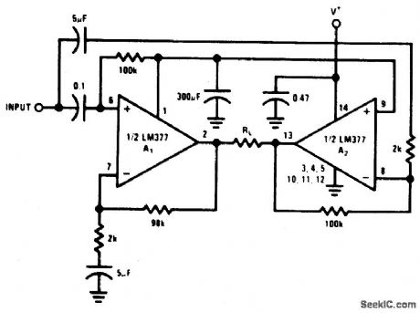
View full Circuit Diagram | Comments | Reading(415)
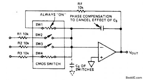
DIGITALLY_CONTROLLED_ONE_OF_FOUR_ANALOG_SWITCH
Published:2009/6/24 3:15:00 Author:Jessie

View full Circuit Diagram | Comments | Reading(1027)
HIGH_GBW_OP_AMP
Published:2009/6/24 3:15:00 Author:Jessie
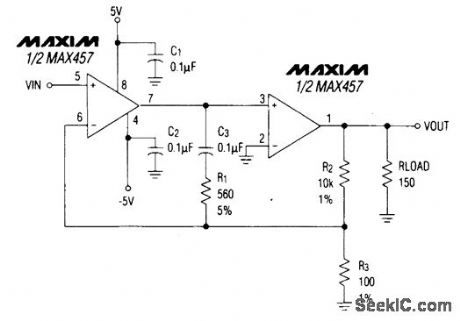
You can build a composite amplifier featuring high gain, wide bandwidth, and good dc accuracy by cascading the sections of a dual video amplifier and adding two appropriate phase-compensation components. The op amp drives a 150-Ω load and provides a closed-loop gain of 40 dB. (View)
View full Circuit Diagram | Comments | Reading(861)
BASIC_ZERO_CROSSING_SWITCH_CIRCUIT
Published:2009/6/24 3:10:00 Author:May

Here is the schematic of a solid-state ac relay with zero-crossing. The triac permits the relay to switch to ac directly. (View)
View full Circuit Diagram | Comments | Reading(0)
INVERTING_POWER_AMPLIFIER
Published:2009/6/24 3:14:00 Author:Jessie

View full Circuit Diagram | Comments | Reading(0)
OSCILLATOR_TRIGGERED_SWITCH
Published:2009/6/24 3:09:00 Author:May

In this circuit (the oscillator-triggered switch), the generated by an astable oscillator. (View)
View full Circuit Diagram | Comments | Reading(0)
RESISTOR_PIN_DIODE_SWITCH
Published:2009/6/24 3:13:00 Author:Jessie

This circuit uses resistors instead of RE chokes to keep costs low. The values of R1 and R2 should be no lower than about 1 kΩ to minimize loss. (View)
View full Circuit Diagram | Comments | Reading(1131)
OP_AMP_AND_ANALOG_SWITCH_RON_COMPENSATOR
Published:2009/6/24 3:08:00 Author:May
This switch is in series with feedback resistor to compensate gain. (View)
View full Circuit Diagram | Comments | Reading(1078)
LOW_OUTPUT_IMPEDANCE_MULTIPLEXER
Published:2009/6/24 3:08:00 Author:May

Both inputs are terminated in their characteristic impedance; 75Ω is typical for video applications. Because the output cables usually are terminated in their characteristic impedance, the gain is 0.5. Consequently, amplifiers U2A and U2B are configured in a gain of +2 to set the circuit gain at 1.R2 and R3 determine the amplifier gain; if a different gain is desired, R2 should be changed according to the equation G = (1 + R3/R2) R5, LCL1, and D1 make up an asymmetrical charge/discharge time circuit that configures U1 as a break-before-make switch to prevent both amplifiers from being ac-tive simultaneously. The multiplexer transition time is approximately 15μs with the component values shown. (View)
View full Circuit Diagram | Comments | Reading(0)
125_MHz_LOGIC_PROBE
Published:2009/6/24 3:06:00 Author:May

This logic probe features either high-low (LED) indication or latching operation. When S1 closed, the indication of a pulse is latched and the red LED1 stays on. Piezoelectric buzzer BZ1 used as a beeper to sound that a logic high is preset. (View)
View full Circuit Diagram | Comments | Reading(0)
ANALOG_SWITCH_CIRCUIT
Published:2009/6/24 3:05:00 Author:May

View full Circuit Diagram | Comments | Reading(679)
ANALOG_SWITCHED_INVERTER
Published:2009/6/24 3:05:00 Author:May

View full Circuit Diagram | Comments | Reading(524)
LONG_TIME_DELAY_MOTOR_CONTROL_CIRCUIT
Published:2009/6/24 3:05:00 Author:May
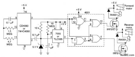
Circuit controls forward and reverse motors.Every hour, one motor runs for 10 seconds. (View)
View full Circuit Diagram | Comments | Reading(884)
ISOLATED_SWITCH
Published:2009/6/24 3:05:00 Author:May

This dc-controlled switch uses an optoisolator/coupler,U1,to electrically isolate the input signalfrom the output control device. (View)
View full Circuit Diagram | Comments | Reading(1200)
SIMPLE_RF_PROBE
Published:2009/6/24 3:05:00 Author:May

Your VTVM can measure peak voltage up to 200 MHz by using this probe. The maximum RF that can be measured is determined by the diode; with a 1N60, the probe is Iimited to 30 V. To increase the capacity, substitute a higher-voltage small-signal detector diode. House the circuit in a metal enclosure and use shielded wire. (View)
View full Circuit Diagram | Comments | Reading(1406)
6_W,8’OHM_OUTPUT_TRANSFORMERLESS_AMPLIFIER
Published:2009/6/24 3:04:00 Author:May
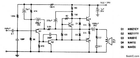
View full Circuit Diagram | Comments | Reading(503)
VARIABLE_GAIN_OP_AMP_CIRCUIT
Published:2009/6/24 3:10:00 Author:Jessie
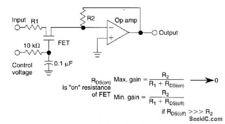
A JFET acts as a variable attenuator for this op amp. Maximum gain is: (View)
View full Circuit Diagram | Comments | Reading(902)
NONLINEAR_OPERATIONAL_AMPLIFIER_WITH_TEMPERATURE_COMPENSATED_BREAKPOINTS
Published:2009/6/24 3:04:00 Author:May
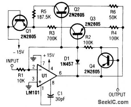
Using resistor and transistor feedback elements, this operational amplifier circuit can be used as a nonlinear amplifier. R4 and R6 can be varied to change breakpoints, as required. (View)
View full Circuit Diagram | Comments | Reading(1138)
| Pages:1348/2234 At 2013411342134313441345134613471348134913501351135213531354135513561357135813591360Under 20 |
Circuit Categories
power supply circuit
Amplifier Circuit
Basic Circuit
LED and Light Circuit
Sensor Circuit
Signal Processing
Electrical Equipment Circuit
Control Circuit
Remote Control Circuit
A/D-D/A Converter Circuit
Audio Circuit
Measuring and Test Circuit
Communication Circuit
Computer-Related Circuit
555 Circuit
Automotive Circuit
Repairing Circuit