
Circuit Diagram
Index 1351
ACCURATE_MOTOR_SPEED_CONTROL
Published:2009/6/24 2:57:00 Author:Jessie

This circuit can control dc motors used in machines that pull materials, such as wire, yam, film, etc., from the supply rolls and rewind them onto smaller rolls. Its motor velocity profile is shown in the figure.A lightweight disk with at least 32 slots is mounted on the motor shaft. It works in a slotted op-tical switch (MOC7811) to sense the motor speed. Phase comparator 2(PC-2)of the phase-locked loop(IC-CD 4046B)compares the frequency (fV)at the output of the VCO with the pulse rate (fm) at the optical switch output. The PC-2 output drives the motor via the transistors when fm>fv, and removes the supply to the motor when fv>fm. The drive system quickly reaches an equilibrium con-dition when fm=fv.Op amps IC-1a, 1b, and 1c form a tracking integrator whose output always smoothly reaches and remains at a voltage equal to the command voltage (Ec) presented at the inverting input of op-amp IC-1a. When the digital control inputs are set to (A=1,B=0=C), the integrator generates a posi-tive slope ramp that sweeps the VCO frequency and, thus, accelerates the motor. The acceleration rate and the constant speed VHI, can be adjusted by presets P4 and PI, respectively.Similarly, when the inputs are set to (A=0=C,B=1), the integrator generates a negative slope ramp that decelerates the motor. Presets P5 and P2 can be adjusted to set the required deceleration and the constant speed VLO, respectively. (View)
View full Circuit Diagram | Comments | Reading(2990)
ADJUSTABLE_POSITIVE_REGULATOR
Published:2009/6/24 2:57:00 Author:Jessie

View full Circuit Diagram | Comments | Reading(1068)
POLARITY_GAIN_ADJUSTMENT
Published:2009/6/24 2:53:00 Author:May

By adjusting one potentiometer, this circuit's output can be varied from a positive-going version of the input signal, smoothly through zero output, then to a negative-going version of the input (see the figure). If the input signal is a positive pulse of, for example, +2-V peak, the output pulse amplitude can be smoothly varied from +2-V through ground (no output) to a -2-V peak.
Taking a closer look at the setup, assume that the signal has a +2-V peak input. The A section of the quad op amp is an input buffer, op amp C provides a fixed negative-going output of -4-V peak, and op amp B supplies a positive-going output that varies from +2-V to +6-V peak. The D section adds the B and C outputs. Thus, by varying the B output, the circuit output varies smoothly from -2-V to +2-V peak.
The circuit can, of course, also be used as a 0°/180° phase switcher. For instance, with a groundcentered sine-wave input of 4V p-p, the output varies from 4-V p-p in phase with the input, smoothly through 0 V, to 4V p-p 180° out of phase with the input. (View)
View full Circuit Diagram | Comments | Reading(827)
STEPPED_TRIANGLE_WAVEFORM_GENERATOR
Published:2009/6/24 2:53:00 Author:May
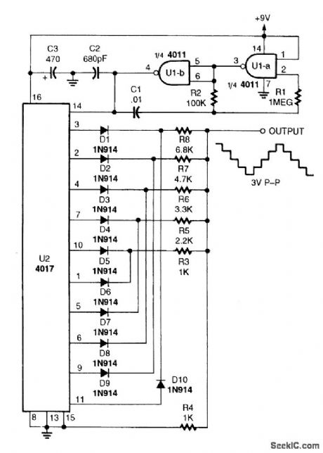
Two gates of a 4011 quad two-input NAND gate (U1) are connected in a pulse generator circuit.The square output at pin 4 of U1-b, connects to the clock input, pin 14, of a 4017 decade counter IC (U2). For each input clock pulse, the 4017 takes a single step. Because the 4017 counter is set up to count ten and then repeat the count, the stepped output frequency will only be Ho of the clock fre-quency. For a 100-Hz output, the clock generator must operate at 1 kHz.The 4017's positive output pulses begin at pin 3 and progress to pin 11 in a serial manner. The first output pulse, at pin 3, passes through Dl and R8 and appears across R4 to produce the first step up the triangle. The second pulse is routed through D2 and R7 to produce the second step. The out-puts at pins 10 and I form the top of the waveform and outputs at pins 5, 6, 9, and 11 produce the down steps. (View)
View full Circuit Diagram | Comments | Reading(4)
SHARP_SQUARE_WAVEFORMS_FROM_MULTIVIBRATOR
Published:2009/6/24 2:50:00 Author:May

By using diodes as shown, the loading effect on the collector of the transistors caused by the tim-irtg capacitors can be avoided. As the collector of the transistors rises toward VCC the diode discon-nects the tinting capacitors. (View)
View full Circuit Diagram | Comments | Reading(0)
SQUARE_WAVE_GENERATOR
Published:2009/6/24 2:50:00 Author:May

A 60-Hz waveform from T1 drives an audio amplifier to clipping. Output is 60 Hz with about 0- to 1.4-V p-p amplitude. (View)
View full Circuit Diagram | Comments | Reading(2)
RECEIVER_AF_NOISE_LIMITER_FOR_LOW_LEVEL_SIGNALS
Published:2009/6/24 2:46:00 Author:May

A preamplifier in the audio frequency range amplifies a noisy audio signal to drive a diode clip-per. Suitable audio input levels would be in the 10-mV to 1-V range. (View)
View full Circuit Diagram | Comments | Reading(0)
GUNSHOT_SOUND_EFFECTS_GENERATOR
Published:2009/6/24 2:46:00 Author:May

Gunshot sound-effects generator built around a Texas Instruments SN76477 sound chip. An in-put pulse causes IC1 to generate a gunshot sound. (View)
View full Circuit Diagram | Comments | Reading(0)
800_Hz_OSCILLATOR
Published:2009/6/24 2:46:00 Author:May

The following transistors may be used: HEP-254, O.C-2, SK-3004, AT30H. To increase the frequency, decrease the value of the capacitors in the ladder network. (View)
View full Circuit Diagram | Comments | Reading(0)
ELECTRONIC_WIND_CHIME
Published:2009/6/24 2:45:00 Author:May

The value of R4 controls the damping or decay time of the feedback circuit (a twin Tee oscillator). When S1 is closed, the circuit breaks into oscillation. When S1 is opened, the circuit stops oscillating generating a decaying tone like a bell.The frequency is approximately 1/2 RC. C1, C2, and C3 are typically in the 0.01-μF range. (View)
View full Circuit Diagram | Comments | Reading(0)
PHASE_SHIFT_OSCILLATOR
Published:2009/6/24 2:45:00 Author:May

A single transistor makes a simple phase shift oscillator. The output is a sine wave with distortion of about 104. The sine wave purity can be increased by putting a variable resistor (25 ohms) in the emitter lead of Q1 (x). The resistor is adjusted so the circuit is only just oscillating, then the sine wave is relatively pure. Operating frequency may be varied by putting a 10 K variable resistor In serles with R3,Or by changing C1,C2,and C3.Making C1,2, 3 equal to 100 nF will halve the operatingfrequency,Operating frequencycanalso bevoltage controlled by a FET In serles with R3,Or optically controlled by an LDR In serles with R3. (View)
View full Circuit Diagram | Comments | Reading(0)
ROBOTIC_CHATTER_SOUND_GENERATOR
Published:2009/6/24 2:44:00 Author:May


This circuit simulates sound effects of a robot, for toy or novelty applications.
(View)
View full Circuit Diagram | Comments | Reading(1741)
AMPLIFIED_NOISE_LIMITER_FOR_SW_RECEIVERS
Published:2009/6/24 2:44:00 Author:May
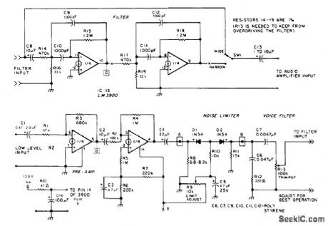
The noise limiter circuit has a preamplifier clipper, and a switchable audio bandpass filter. Audio levels in the 5- to 50-mV range are amplified in a preamp to several volts p-p, fed to a clipper, voice band filter, then to a narrow band active filter which can be switched in and out of the circuit. (View)
View full Circuit Diagram | Comments | Reading(2813)
BIRD_CHIRP_SOUND_EFFECT_GENERATOR
Published:2009/6/24 2:42:00 Author:May
A low-frequency oscillator modulates a higher frequency oscillator, which drives the speaker. (View)
View full Circuit Diagram | Comments | Reading(1116)
ELECTRONIC_WHISTLE
Published:2009/6/24 2:42:00 Author:May

The circuit shown is a twin-tee oscillator. R1 varies the pitch, R2 the duration, and R3 the for-mat (bell, rise 8u fall time, etc.). Vary R4, R5, C4 and C2, C3 for large shifts in frequency. (View)
View full Circuit Diagram | Comments | Reading(769)
AUDIO_DYNAMIC_NOISE_REDUCTION_SYSTEM
Published:2009/6/24 2:41:00 Author:May

U1 is a dedicated IC (National Semiconductor) that achieves up to adaptive bandwidth scheme and a psycho acoustic masking technique. (View)
View full Circuit Diagram | Comments | Reading(1405)
SURF_MAN_SOUND_GENERATOR
Published:2009/6/24 2:41:00 Author:May

Three low-frequency oscillators (IC1d, e, f) are used to simulate wave action of the surf. Q1 is an emitter-base junction used as a diode noise generator, biased by dc derived from oscillator ICl-c.The noise is fed into two voltage-controlled filters R22, R23, C12, C13, with D3 and D4 as tuning elements. The low-frequency oscillator signals randomly vary the filters, therefore, the spectrum of the noise signal fed through them. This simulates the sound of a surf. (View)
View full Circuit Diagram | Comments | Reading(878)
VARIABLE_VOLTAGE_REGULATOR_WITH_CURRENT_CROWBAR_LIMITING
Published:2009/6/24 2:40:00 Author:May


The variable voltage regulator with current-crowbar limiting, shown in Fig. 71-1A, overcomes the disadvantages of constant and foldback limiting. As you can see in the graph (Fig. 71-1B), the current crowbar quickly shuts down the supplied power when a preset current is exceeded. It also has excellent load regulation over its operating range. (View)
View full Circuit Diagram | Comments | Reading(1121)
ADJUSTABLE_POWER_SUPPLY
Published:2009/6/24 2:53:00 Author:Jessie

Using an LM317, this supply delivers 1.25 to 22 Vdc for various purposes. The LM317 should be heatsinked. This supply will deliver 600-mA output current. (View)
View full Circuit Diagram | Comments | Reading(1136)
TRANSCEIVER_POWER_SUPPLY_FOR_VARIABLE_LAB_SOURCE
Published:2009/6/24 2:51:00 Author:Jessie

A variable voltage regulator provides 1 to 11 Vdc for lab bench work,using an existing 13.8-V transceiver supply. (View)
View full Circuit Diagram | Comments | Reading(3932)
| Pages:1351/2234 At 2013411342134313441345134613471348134913501351135213531354135513561357135813591360Under 20 |
Circuit Categories
power supply circuit
Amplifier Circuit
Basic Circuit
LED and Light Circuit
Sensor Circuit
Signal Processing
Electrical Equipment Circuit
Control Circuit
Remote Control Circuit
A/D-D/A Converter Circuit
Audio Circuit
Measuring and Test Circuit
Communication Circuit
Computer-Related Circuit
555 Circuit
Automotive Circuit
Repairing Circuit