
Circuit Diagram
Index 1361
12_Vdc_REGULATED_SUPPLY
Published:2009/6/23 4:48:00 Author:Jessie

View full Circuit Diagram | Comments | Reading(591)
MODULATOR_FOR_VIDEO
Published:2009/6/23 4:47:00 Author:Jessie

This circuit uses an LM2889 and a saw filter for use as a TV modulator. (View)
View full Circuit Diagram | Comments | Reading(549)
Motor vehicle steering light controller 1
Published:2011/7/29 3:06:00 Author:Ecco | Keyword: Motor vehicle, steering light controller

(View)
View full Circuit Diagram | Comments | Reading(470)
TWO_PHASE_RECTIFIER
Published:2009/6/23 4:21:00 Author:May

The waveform generated by the two-phase rectifier illustrates that the ripple is less than half that of a conventional single-phase circuit's wavefrom. Also,the ripple frequency is double that of the conventional circuit. The circuit amplitude changes in the ac input signal very rapidly,and it works equally will with current or voltage inputs. (View)
View full Circuit Diagram | Comments | Reading(686)
SINUSOIDAL_3_Hz_TO_300_kHz_VCO
Published:2009/6/23 4:15:00 Author:May
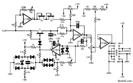


This circuit uses Analog Devices' AD639 universal trigonometric function generator to convert a triangle waveform, the basic waveform of the VCO itself, into a very low-distortion sine wave.By using the AD639 in its frequency tripler mode [2], the frequency range 3 Hz to 300 kHz is now covered. The circuit has been drawn here so that the oscillator loop, consisting of Q1, the integrator and the LT1011 comparator, is clearly shown.When Q1 is off, the input amplifier, which is adjusted to have a gain of exactly -1, pulls a current VIN/R, where R is 5.1 kΩ in series with two JFETs, and Q2 and Q3, out of the virtual earth of the in-tegrator. The output of the integrator thus rises at a rate of VIN/CR, where C = 470 pF. At a level that can be adjusted by the 5-kΩ potentiometer, the comparator flips and turns on Q1.A current of exactly 2VIN/R, is now supplied to the virtual earth of the integrator because there are now two 5.1-kΩ resistors in parallel and only a single JFET in between the virtual earth and Vin.The integrator output now falls at a rate of VIN/CR and the cycle repeats. Any offset in the current to the virtual earth of the integrator, due to circuit board leakage, etc., can be corrected by adjusting the 50-kΩ potentiometer. It follows that the symmetry of the triangle wave at the integrator output can be corrected by adjusting the 2-kΩ potentiometer, and the 50-kΩ potentiometer at VLF, and the frequency can be trimmed with the 5-kΩ potentiometer.The l-kΩ potentiometer variable is adjusted to give the input level to the AD639 needed to drive it over ±270°and so produce a sinusoidal output at three times the frequency of the triangle-wave input. Offset correction for the AD639 is made at the input to the voltage follower by means of the 20-kΩ potentiometer.Once a symmetric triangle wave has been obtained by adjusting the 2-kΩ and 50-kΩ poten-tiometers, and the correct frequency of 100 kHz has been set for VIN/=10 V, by adjusting the 5-kΩ potentiometer, the triple-frequency she-wave output can be set up by adjustment of the 1-kΩ and 20-kΩ potentiometers.This is best done by triggering the CRO from the triangle wave, and then viewing at least three complete cycles of output. Having adjusted for a clean-looking sine wave, the final adjustment of the 1-kΩ and 20-kΩ potentiometers should be made on a single sinusoidal cycle display, using internal trigger so that the three slightly different parts of the output cycle lie one upon the other and can be made to merge. Q1, Q2, and Q3 are 2N4391s, the two Schottlqr diodes are 5082-2810, and the other nine diodes are 1N914.All device power supply pins should be decoupled with 0.33 p.F. Resistors associated with the in-puts of the devices should be 1% high-stability parts. (View)
View full Circuit Diagram | Comments | Reading(2975)
Motor vehicle steering flasher 2
Published:2011/7/29 3:05:00 Author:Ecco | Keyword: Motor vehicle , steering flasher
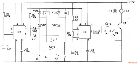
The motor vehicle steering flasher described in the example controls left and right turn signal by two control buttons respectively. Clicking the button will automatically turn on lights (one flash per second), it flashes about 20S then automatically turns off the power supply, thus avoiding the traffic accidents caused by forgetting to turn off lights.
The working principleThe motor vehicle steering flasher circuitis composed of monostable delay trigger, multivibrator and the trigger control circuit, it is shown as the chart 7-24.
Monostable circuitis composed of the time base trigger delay circuit ICl, resistors Rl, R2, capacitor Cl, C2.
Multivibrator integrated circuitis composed ofthe time base IC2, resistors R3, R4 and capacitors C3, C4.
Control circuit is composed of the control button Sl, S2, the relay Kl, K2, transistors Vl, V2 and diode VDl-VD6.
Component selection
Rl-R4 select the 1/4W metal film resistors or carbon film resistors; R5 selects the1W metal film resistor.
C uses the aluminium electrolytic capacitor with the voltage in 25V; C2 and C4 choose the monolithic capacitors or polyester capacitors.
Vl and V2 select 3DDl5 or DDO3 NPN silicon transistors. (View)
View full Circuit Diagram | Comments | Reading(500)
Battery Charging Circuit of MAX1737
Published:2011/7/23 2:13:00 Author:Michel | Keyword: Battery Charging Circuit

The above picture is battery charging circuit of MAX1737.There is PWM type synchronous rectifier step-down transformation circuit inside MAX1737.Its input voltage is 28 V and switch frequency is 300 kHZ. It has all funtions that charging circuit needs,namely,the input current monitoring, battery temperature monitoring, battery fault dindictaion, charging termination and the timing charging functions, etc.
MAX1737 tube feet functions are as follows.1 feet (VL)-The work power is input in DCIN port and this port is 5.4 V linear regulators output. Feet 2(ISETIN)-the input current limited port. (View)
View full Circuit Diagram | Comments | Reading(1879)
TWO_TERMINAL_100_mA_CURRENT_REGULATOR
Published:2009/6/23 4:14:00 Author:May

The circuit has a low temperature coefficient and operates down to 3 V. The reverse base current of the LM195 biases the circuit.
A 2N2222 is used to control the voltage across current-sensing resistor, R2 and diode D1, and therefore the current through it. The voltage across the sense network is the VBE of the 2N2222 plus 1.2 V from the LM113. In the sense network, R2 sets the current and D1 compensates for the VBE of the transistor. Resistor R1 sets the current through the LM113 to 0.6 mA. (View)
View full Circuit Diagram | Comments | Reading(712)
5_V_LOGlC_REGULATOR_WITH_ELECTRONIC_SHUTDOWN
Published:2009/6/23 4:47:00 Author:Jessie

The circuit will shut down to 1.2 V under fault conditions. (View)
View full Circuit Diagram | Comments | Reading(607)
Vehicle flashing lights controller 5
Published:2011/7/29 2:55:00 Author:Ecco | Keyword: Vehicle, flashing lights, controller

The motor vehicle flashing lights controller described in the example is composed of LED light-emitting diodes and control circuit.It can be installedin the rear window of the motorcycle or car, when driving at night, the light-emitting diode is lit like the water cycle; It can grasp people's attention.
Working principle
The motor controller circuit is composed of the LED drive circuit and oscillator, it is shownas Figure 7-29.
When the voltage of the two ends of C is lower than 3.4V, which is the reference voltage of N2, the output of N2-N8 is in low level, VLl-VLl8 are off.
When the voltage of the two ends of C ishigher than 43V, the output of N2 is in low level, and the output of N3 is in high level,VLl-VL3 are off, VL7-VL9 are on.
When the voltage of the two ends of C ishigher than 5.2V, the output of N3 is in low level, and the output of N4 is in high level,VL4-VL6 are off, VL7-VL9 are on.
When the voltage of the two ends of C ishigher than 6V, the output of N4 is in low level, and the output of N5 is in high level,VL7-VL9 are off, VL0-VL2 are on.
When the voltage of the two ends of C ishigher than 6.8V, the output of N5 is in low level, and the output of N6 is in high level,VL0-VL2 are off, VL3-VL5 are on.
When the voltage of the two ends of C ishigher than 7.7V, the output of N6 is in low level, and the output of N7 is in high level,VL3-VL5 are off, VL6-VL8 are on. (View)
View full Circuit Diagram | Comments | Reading(536)
SIMPLE_dc_ac_INVERTER
Published:2009/6/23 4:46:00 Author:Jessie

This dc-to-ac inverter is based on the popular 555. A 555 oscillator circuit drives a buffer amplifier consisting of Q1, Q2, and Q3. The circuit operates at 150 to l60 Hz. T1 can be a 6.3-V or l2.6-V ffia-ment transformer as applicable. The frequency canbe changed by changing the values of R1 and/or C1. (View)
View full Circuit Diagram | Comments | Reading(8053)
OP_AMP_AUDIO_MIXER
Published:2009/6/23 4:13:00 Author:May

This circuit will mix several audio signals to a common output.RF can be made 1 MΩ for 10 ×(20dB) or 100kΩ for unity gain. (View)
View full Circuit Diagram | Comments | Reading(1210)
FAST_33_V_ADJUSTABLE_REGULATOR
Published:2009/6/23 4:12:00 Author:May


The adjustable version of the LT1585 makes it relatively easy to accommodate multiple microprocessor power-supply voltage specifications. To retain the tight tolerance of the LT1585 internal reference, a 0.5% resistor adjustment is recommended. R1 is sized to carry approximately 10 mA idling current (≤124 Ω), angl R2 is calculated from: (View)
View full Circuit Diagram | Comments | Reading(525)
The Numerical Control DC Regulated Power Supply Circuit 6
Published:2011/7/22 21:55:00 Author:Michel | Keyword: Numerical Control, DC Regulated Power Supply

The control DC regulated power supply circuit introduced in the example uses light touch buttons and digital integrated circuit to control the output low voltage of voltage regulation circuit.Its output voltage range is 1.5-30V.The circuit uses 20 reversible gears stepping control(stepping value is 1.5V).The low voltage gear is 1.5-15V(zero to ninth gear) and high voltage gear is 16.5-30V(tenth to ninth gear) and the output votage gear is indicated by LED digital display.
Circuit's Work PrincipleThis control DC regulated power supply circuit is composed of voltage regulation circuit,control circuit and gear indication circuit and it is showed as the picture 5-25.
Voltage regulation circuit consists of mains switch,S1,gear selector switch,S2a ,FU1-FU3,mains transformer,T, rectifier diode ,VD10,capacitor,C1-C7,voltage regulator IC,IC4 and resistor,RO. (View)
View full Circuit Diagram | Comments | Reading(858)
TWO_TONE_SIREN
Published:2009/6/23 4:45:00 Author:Jessie

IC1 generates the main siren tone while IC2 generates a low-frequency square wave, switching IC1 between two different tones. (View)
View full Circuit Diagram | Comments | Reading(0)
The gas overranging alarm miner lamp 1
Published:2011/7/29 2:57:00 Author:Ecco | Keyword: gas overranging , alarm , miner lamp

The gas overranging alarm miner lamp described in the example is suitable for the environment with explosion gas in coal mine, the miners carry the device for lighting and detecting methane gas. When the methane gas is overlimit, the alarm signal will flash in time to remind miners to evacuate in time.
The working principle:The gas overranging alarm miner lamp circuit is composed of detection amplifier circuit and alarm circuit. It's shown as the figure 8-29.
The detection amplifier circuit is composed of sensor, resistors Rl-Rl5, potentiometer RP, transistors Vl-V7 and voltage regulator diode VS. The alarm circuit consists of resistors R16-Rl8, capacitors Cl-C4, transistors V8 and V9, Diodes VDl and VD2, the relay K and miner's lamp EL.Turning on the power switch S (Sl, S2), EL is lit, the entire circuit gets power supply. The end of the sensor detects methane gas, the internal resistance of pure white carrier elements B and black catalytic elements A in sensor keep stable, V6 and V7 is off, the oscillator composed of V8, V9, and Cl-C4, R16-R18, K , VDl stops vibrating, K is in releasing state, EL in normal lighting condition.
(View)
View full Circuit Diagram | Comments | Reading(617)
BUFFERED_REFERENCE_SUPPLY
Published:2009/6/23 4:45:00 Author:Jessie
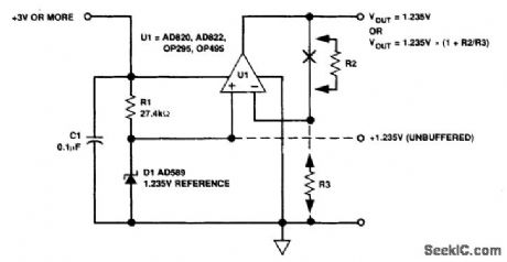
This buffered reference (for 1.23 V or ntore) uses a supply voltage of greater than 3 V. (View)
View full Circuit Diagram | Comments | Reading(432)
REGULATOR_CIRCUIT_FOR_BILATERAL_SOURCE_LOAD_POWER_SYSTEM
Published:2009/6/23 4:10:00 Author:May

The figure shows a circuit that regulates an output voltage, regardless of the direction of flow of output current. More specifically, it regulates the voltage at the left source or load, which can either supply power to or receive power from the right load or source, depending on the voltages and the direction of flow of current at the load/source terminals.The overall system can be characterized as a voltage-controlled current source with bilateral current capability. The current flowing between the two source/loads, averaged over a power-switching cycle, is made to depend on the pulse-width modulation that governs the operation of the two power-switching devices, and this pulse-width modulation is, in turn, a function of amplified currenterror and voltage-error signals. The voltage error is the difference between the actual output voltage and the output-reference voltage, which is the nominal output voltage at zero current. The pulsewidth modulation is varied to increase or decrease the current, as needed, to limit the excursion of output voltage from the reference value.An additional feature of this control circuit is that the maximum current in either direction can be limited by limiting the excursion of the output voltage from the zero-current value. Thus, external current-limiting circuitry is not necessary. (View)
View full Circuit Diagram | Comments | Reading(595)
dc_dc_CONVERTER
Published:2009/6/23 4:45:00 Author:Jessie

This low-power converter will supply about 100 mW of dc to a load and it is useful to isolate or derive dc voltages. It operates at around 200 kHz. L1 is wound on a 22-mm diameter x 13-mm high pot core with #32 magnet wire. The primary is 80 turns and the secondary is 80 turns (for 12-V nom-inal output). The two windings should be insulated for the expected voltage difference between in-put and output in insulation applications. (View)
View full Circuit Diagram | Comments | Reading(1)
Monolithic Voice Record-replay Intergarted Circuit
Published:2011/7/22 21:38:00 Author:Michel | Keyword: Monolithic Voice Record-replay , Intergarted Circuit

Monolithic Voice Record-replay Intergarted Circuit
QX-R42 can constitute a monolithic solid recorder and its sentence is input by users and played repeatedly.Please press button SA3 when you record and at the time,27 feet of the IC is in low PWL and voice signals enter storage unit via Microphnone,MIC.Plesae loosen the button and it can play the voice after finishing recording.There are two palyback buttons.SA1 is low PWL triggering playback.SA2 caues tirggering playback by pulse falling.SA1 can be chosen and SA2 is not used when we choose playback button.When we choose to use other circuit'spulsetriggering but button and the pulse will be input IC's 24 feet and it constitute automatic playback mode.LED is recording indicating light and it sparks during the recording process.R5 and R6 constitute automatic gain control net.R2 and C3 constitute analog signals which iuput and output coupling loop.Thus the 14th and 15th feet output playback signals and the speaker is drived to playback directly. (View)
View full Circuit Diagram | Comments | Reading(667)
| Pages:1361/2234 At 2013611362136313641365136613671368136913701371137213731374137513761377137813791380Under 20 |
Circuit Categories
power supply circuit
Amplifier Circuit
Basic Circuit
LED and Light Circuit
Sensor Circuit
Signal Processing
Electrical Equipment Circuit
Control Circuit
Remote Control Circuit
A/D-D/A Converter Circuit
Audio Circuit
Measuring and Test Circuit
Communication Circuit
Computer-Related Circuit
555 Circuit
Automotive Circuit
Repairing Circuit