
Circuit Diagram
Index 1366
BABY_MONITOR
Published:2009/6/23 3:31:00 Author:Jessie

Transmitter operation. Operating power for the transmitter circuit is derived directly from the ac line. The dc power to operate the circuit is generated in two stages, one for an RE power-amplifier stage, and the second for the remainder of the circuit.
The ac line voltage is applied to D1 , which half-wave rectifies the ac input . The resulting dc voltage (approximately 30V under load) is fed across an RC filter (comprised of R1 and C1) and used to operate amplifier, Q1. The second stage of the power supply (composed of LED1, R2, D2, D3, C2, and C3, which forms a regulated +13.6-V, center-tapped supply) feeds the remainder of the circuit. LED1 is connected in series with R2 and is used as a visual power-on indicator for the transmitter.
An electret microphone element (MIC1) is used as the pick-up. The output of the microphone is ac coupled through C5 to UI-a (a noninverting op amp with a gain of about 100). The output of U1-a at pin 1 is ac coupled through C4 to the noninverting input of UI-b (which provides an additional gain of 48) at pin 5. The output of UI-b at pin 7 is then fed through D4 and RIO, and across R11 and C6 to the inverting input of UI-c which is biased to a positive voltage that is set by SENSITIVITY-control R19. This represents a threshold voltage at which the output of UI-c switches from high to low.
During standby, the output of UI-c at pin 8 is held at about 12 V when the voltage developed across C6 is less than the bias-voltage setting at pin 10. When a sound of sufficient intensity and du-ration is detected, the voltage at pin 9 of UI-c exceeds the threshold level (set by R19), causing UI-c's output at pin 8 at go low. That low is applied to pin 2 of U2 (a 555 oscillator/timer configured as a monostable multivibrator). This causes the output of U2 to go high for about one second, as de-termined by the time constant of R12 and C7. The output of U2 at pin 3 is applied to pin 4 of U3 (a second 555 oscillator/timer that is conftgured for astable operation, with a frequency of about 125 kHz). That causes U3 to oscillate, producing a near square-wave output that is used to drive Q1 into conduction. The output of Q1 is applied across a parallel-tuned circuit composed a T1's primary and C8. The tuned circuit, in turn, reshapes the 125-kHz signal, causing a sine-wave-like signal to appear across both the primary and the secondary of Tl.
The signal appearing at T1's secondary (about 1 or 2 V peak-to-peak) is impressed across the ac power line, and is then distributed throughout the building without affecting other electrical appli-ances connected to the line. Transient suppressor D7 is included in the circuit to help protect Q1 from voltage spikes that might appear across the power line and be coupled to the circuit through T1.
Receiver operation. Power for the receiver, as with the transmitter, is derived from a tradi-tional half-wave rectifier (D5). The resulting dc voltage is regulated to 27 V by D6 and R20, and is then filtered by C11 to provide a relatively clean, dc power source for the circuit. A light-emitting diode, LED2, connected in sGries with R20 provides a visual indication that the circuit is powered and ready to receive a signal.
The 125-kHz signal is plucked from the ac line and coupled through R21 and C12 to a parallel-tuned LO circuit, consisting of C13 and L1. That LO circuit passes 125-kHz signals while attenuating all others. The 125-kHz signal is fed through C14 to the base of Q2 (which is configured as a high-gain linear amplifier), which boosts the relatively low amplitude of the 125-kHz signal. The RE out-put of Q2 is ac coupled to the base of Q3 through C15. Transistor Q3 acts as both an amplifier and detector. Because there is no bias voltage applied to the base of Q3, it remains cut off until driven by the amplified 125-kHz signal. When Q3 is forward biased, its collector voltage rises.
Capacitor C16, connected across Q3's collector resistor, filters the 125-kHz signal so that it is essentially dc. When the voltage at the collector of Q3 rises, Q4 is driven into conduction. That causes current to flow into piezo buzzer BZ1, producing a distinctive audio tone that alerts anyone within earshot that the baby needs attention. (View)
View full Circuit Diagram | Comments | Reading(2778)
AUDIO_DISTRIBUTION_AMPLIFIER
Published:2009/6/23 3:24:00 Author:May

View full Circuit Diagram | Comments | Reading(0)
INVERTING_AMPLIFIER
Published:2009/6/23 3:31:00 Author:Jessie

View full Circuit Diagram | Comments | Reading(1335)
FOLDBACK_CURRENT_LIMITER
Published:2009/6/23 3:23:00 Author:May

This regulator uses the drop across R3 to sense current draw, turning on Q2, removing drive from Q1, and lowering the output voltage. Limiting occurs when Q2 has 0.65 V across the base-emitter junction. This circuit has foldback characteristics as seen from the figure. (View)
View full Circuit Diagram | Comments | Reading(1)
MASTER_SLAVE_DEVICE_ERROR_CHECKER
Published:2009/6/23 3:30:00 Author:Jessie

An error-check mechanism introduced into master and slave communication devices can indi-cate mismatches when both the master and slave start sending data simultaneously. The error ftag goes high and indicates a mismatch in the data.The master is the one that can interrupt the communication from a device at the other end and force it to listen. It does this forcing a low voltage level over the communication line by raising the control line to a high level. This inhibits data flow over the tines from the slave device. As a result, the slave turns into a listen mode(not a hardware feature, but rather incorporated in the software). The slave device can transmit the data after communication from the master device ceases. (View)
View full Circuit Diagram | Comments | Reading(1531)
×10_FREQUENCY_MULTIPLIER
Published:2009/6/23 3:23:00 Author:May

In this circuit, the CD4046 is set up so that the VCO operates at 10 to 100 kHz. The output pin(4) is fed back to a ÷10 counter. When the input frequency is 1/10 the output, lockup will occur. (View)
View full Circuit Diagram | Comments | Reading(3051)
LOG_RATIO_AMPLIFIER
Published:2009/6/23 3:30:00 Author:Jessie
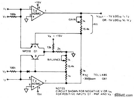
View full Circuit Diagram | Comments | Reading(845)
SIGNAL_DISTRIBUTION_AMPLIFIER
Published:2009/6/23 3:23:00 Author:May
View full Circuit Diagram | Comments | Reading(610)
LOW_VOLTAGE_POWER_CONTROLLER
Published:2009/6/23 3:19:00 Author:May

The circuit has a duty-cycle generator that will produce an output varytng from fully off to fully on and pulses of any duty cycle in between the two extremes.This method of operation is called PWM (pulse zuidth moduhtion) The circuit can be fed fromany dc supply source of between 10 to 15 V Half of an LM556 dual oscillator/timer and U2 a(1/4 of an LM339 quad comparator) combine to form a voltage to-pulse-width converter The first half of thedual os dilator/timer(U1-a) is configured as an astable oscillator,generating a continuously oscillating ramp voltage Op amp U2-a compares the voltage at its noninverting input (pin 5)—which is connected to pins 2 and 6 of U1-a—to the voltage at its inverting input(pin 4) The op amp will producea low output f R1’s wiper voltage lb higher than the instantaneous voltage that is present at pins 2 and 6 of U1-a,The output of U2-a at pin 2 will have an on/off ratio that is proportional to the voltageat R1's wiper.The output of U2-a is fed to U1-b,which is used to buffer the signal,The low-impedance,pulsedoutput of U1-b at pin 9 is fed to the gate of MOSFET Q1,driving it on or off The circuit also has apower-input detector,built around U2-band and LED1. If the input power is OK,LED1 will shut off.Diode D1 is used to Suppress the reverse voltage spikes that are generated by inductive loads during turn off;without that diode,the MOSFET might be destroyed.If the circuit will not be usedto drive inductive loads(motors),D1 can be eliminated. (View)
View full Circuit Diagram | Comments | Reading(2301)
POSITIVE_FEEDBACK_CABLE_TERMINATOR
Published:2009/6/23 3:18:00 Author:May

Positive feedback along with a series output resistor can provide a controlled output impedance from an op-amp circuit. The circuit is useful when driving coaxial cables that must be terminated at each end in their characteristic impedance, which is often 50Q. Adding a 50-Q series resistor on the op amp's output obviously reduces the available signal swing. (View)
View full Circuit Diagram | Comments | Reading(0)
Level 4 Telecom Filter Circuit of uA741 Op-amp
Published:2011/7/22 21:56:00 Author:Michel | Keyword: Op-amp, Level 4, Telecom, Filter Circuit

The above circuit can use common calculation formula and then the total requirements are divided into several sections:Q1=0.541,Q2=1.306.This circuit adopts LM148 or 741 four operational amplifier. (View)
View full Circuit Diagram | Comments | Reading(882)
ROOM_MONITOR
Published:2009/6/23 3:17:00 Author:May

The circuit uses Q1 to buffer the right-channel balance output while Q2 and Q3 form a VOX circuit. When the signal level from the microphone goes high, the output of the VOX also goes high and the multiplexer inside IC1 switches the high-gain left-channel output through to a following buffer stage. This signal is then ac-coupled via C3 into an RE mixer stage and thence to an RF amplifier, which is tuned by C2 and L2. (View)
View full Circuit Diagram | Comments | Reading(0)
455_kHz_MODULATOR
Published:2009/6/23 3:10:00 Author:May

This circuit shows how to frequency-modutate the oscillator using a 555. Oscillator frequency is set with the 5-kΩ potentiometer and the modulation signal is dc-coupled. (View)
View full Circuit Diagram | Comments | Reading(0)
FM_MODULATOR
Published:2009/6/23 3:08:00 Author:May

The FM modulator is built with a Motorola MC1648P oscillator. Two varactors, Motorola MV209, are used to frequency modulate the oscillator. The 5000-Ω potentiometer is used to bias the varactors for best linearity. The output fre-quency of approximately 100 MHz can be ad-justed by changing the value of the inductor. The output frequency can vary as much as 10 MHz on each side. The output level of the modulator is -5 dBm. In this prototype, the varactor bias was 7.5 V for best linearity; but this could be different with other varactors. (View)
View full Circuit Diagram | Comments | Reading(0)
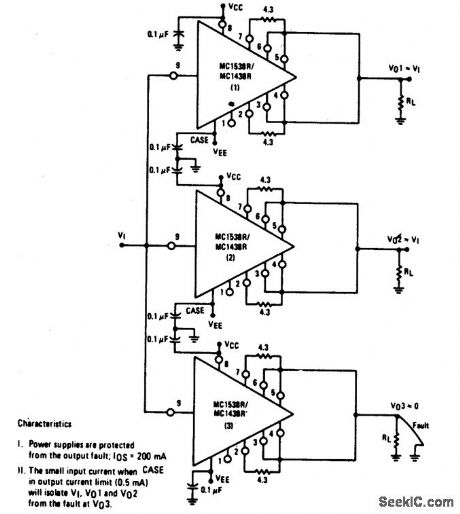
IC_REGULATOR_PROTECTION
Published:2009/6/23 3:55:00 Author:Jessie

This circuit protects an IC regulator against various fault conditions. (View)
View full Circuit Diagram | Comments | Reading(1906)
POWER_SUPPLY_FOR_HIGH_POWER_AUTOSOUND_AMP
Published:2009/6/23 3:53:00 Author:Jessie

A switching mode inverter is used with a pulse-width modulation voltage regulator (SG35260).Four IRF240 power MOSFETs are used as switches. The output is ±47 V at about 5 A peak. Transformer T101 is a four-turn center tapped primary, and 16-turn center tapped secondary on a Ferrox cube ETD-34 core. (View)
View full Circuit Diagram | Comments | Reading(3832)
ac_POWER_LINE_MONITOR
Published:2009/6/23 3:07:00 Author:May

When the power-line voltage source fails,Q1 turns on,activates optoisolator U2, and triggers SCR1.For small SCRs,U1 might directly trigger SCR1. (View)
View full Circuit Diagram | Comments | Reading(0)
SIMPLE_AUDIO_MIXER
Published:2009/6/23 3:45:00 Author:Jessie

A single transistor is used as an audio mixer, the transistor serving as a feedback amplifier. (View)
View full Circuit Diagram | Comments | Reading(1196)
FAST_33_V_REGULATOR
Published:2009/6/23 3:45:00 Author:Jessie


New high-performance microprocessors require a fresh look at power-supply transient response.The LT1585 linear regulator features 1% initial accuracy, excellent temperature drift and load regulation, and virtually perfect line regulation. Complementing superb dc characteristics, the LT1585 exhibits extremely fast response to transients. Transient response is affected by more than the regulator itself. Stray inductances in the layout and bypass capacitors, as well as capacitor ESR dominate the response during the first 400 ns of transient.The ftgure shows a bypassing scheme developed to meet all the requirements for the Intel P44C-VR microprocessor. Input capacitors C1 and C2 function primarily to decouple load transients from the 5-V logic suppJy. The values used here are optimized for a typical 5-V desktop computer silver box powersupply input. C5 to C10 provide bulk capacitance at low ESR and ESL, and C11 to C20 keep the capacitance at low ESR and ESL low at high (>100 kHz) frequencies. C4 is a damper and it minimizes ringing during setting. Trace C is the load current step, which is essentially flat at 4 A with a 20-ns rise time.Trace A is the output settling response at 20 mV per division. Cursor trace B marks -46 mV relative to the initial output voltage. At the onset of load current, the microprocessor socket voltage dips to -38 ntV as a result of inductive effects in the board and capacitors, and the ESR of the capacitors. The inductive effects persist for approximately 400 ns. For the next 3 μs, the output droops as the load current drains the bypass capacitors. The trend then reverses as the LT1585 catches up with the load demand, and the output settles after approximately 50 μs. Running 4 A with a 1.7-V drop, the regulator dissipates 6.8 W. (View)
View full Circuit Diagram | Comments | Reading(1383)
SIMPLE_FLOOD_ALARM
Published:2009/6/23 3:43:00 Author:Jessie

A common collector amplifier drives a 2N3904 switch to sound alarm BZ1. The wire leads to wa-ter sensor or surnp pit, level switch, etc. and used to allow the alarm to operate and be mounted in a dry place. (View)
View full Circuit Diagram | Comments | Reading(1683)
| Pages:1366/2234 At 2013611362136313641365136613671368136913701371137213731374137513761377137813791380Under 20 |
Circuit Categories
power supply circuit
Amplifier Circuit
Basic Circuit
LED and Light Circuit
Sensor Circuit
Signal Processing
Electrical Equipment Circuit
Control Circuit
Remote Control Circuit
A/D-D/A Converter Circuit
Audio Circuit
Measuring and Test Circuit
Communication Circuit
Computer-Related Circuit
555 Circuit
Automotive Circuit
Repairing Circuit