
Circuit Diagram
Index 1370
BOOTSTRAP_CIRCUIT
Published:2009/6/23 2:33:00 Author:May

Bootstrapping the substrate of a JFET amplifier reduces the distortion caused by the nontinlearity of the JFET input capacitance. In the figure, a second feedback divider bootstraps the substrate of U1. With R1=500 kΩ (source im-pedance), THD at 10 kHz was reduced an order of magnitude. (View)
View full Circuit Diagram | Comments | Reading(1382)
CLAPP_OSCILLATOR_FOR_100_kHz
Published:2009/6/23 2:32:00 Author:May
This Colpitts oscillator is very stable and usable where good stability is needed, but crystal control is not desirable. It is capable of 1 part in 104 to 105 with good-quality components. (View)
View full Circuit Diagram | Comments | Reading(901)
COLPITTS_OSCILLATOR
Published:2009/6/23 2:31:00 Author:May
In this circuit, the oscillator is free-running. (View)
View full Circuit Diagram | Comments | Reading(0)
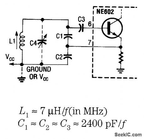
OSCILLATOR_CIRCUITS
Published:2009/6/23 2:31:00 Author:May

These are methods of using an NE602 with a tunable VFO. (View)
View full Circuit Diagram | Comments | Reading(1196)
“UNIVERSAL”VFO
Published:2009/6/23 2:30:00 Author:May

Figure 63-16A shows the basic circuit for the VFO, except for the tuning circuits (which are shown in Fig. 63-16B). Transistor Q1 is a junction field-effect transistor (JFET) oscillator stage. The device to use at Q1 includes MPF-102, 2N4416, and the replacement devices from the popular lines of service parts e.g., ECG and NTE).Two different oscillator configurations can be accommodated by this design (i.e., both Clapp and Colpitts oscillators can be built). Both oscillators are the same from point A in Fig. 63-16C forward, and both depend on a capacitor voltage-divider feedback network. The Clapp oscillator (Fig. 63-16A) is series-tuned and the Colpitts oscillator is parallel-tuned (Fig. 63-16B).The dc voltage supplied to the oscillator transistor (Q1) is voltage-regulated. The voltage regu-lator can be any 78Lxx series from 78LO5 to 78LO9. (View)
View full Circuit Diagram | Comments | Reading(3184)
Sine wave signal source with stable output
Published:2011/7/28 3:24:00 Author:Ecco | Keyword: Sine wave , signal source , stable output

Figure shows the sine wave signal source with stable output. First using of an op amp comparator could produce a constant 60Hz square wave. The output end of comparator is connecting to a pair of 6.2V back connecting zener diodes. The following is a two-stage Sallen-key low pass filter, which canfilter out all harmonics. Capacitive coupling amplifier cuts off the DC component produced by zener diode which is not equal in circuit, it also make compensation for filter loss, and the precise calibration of the output amplitude can reach l0V peak. The result is that it gets a high stable 60Hz sine wave voltage with low distortion. In the case of constant ambient temperature, power supply voltage range is 90 ~ 135V, the sine wave output voltage rate of change is less than 5mV.
(View)
View full Circuit Diagram | Comments | Reading(793)
SIMMAX card reader principle diagram
Published:2011/7/25 3:05:00 Author:Ecco | Keyword: SIMMAX , card reader, principle diagram

View full Circuit Diagram | Comments | Reading(1472)
PC remote control circuit
Published:2011/7/25 3:02:00 Author:Ecco | Keyword: PC , remote control

View full Circuit Diagram | Comments | Reading(693)
The design of dot matrix LED electronic display
Published:2011/7/25 3:04:00 Author:Ecco | Keyword: design , dot matrix, LED , electronic display

H1 ~ H16 can choose 8550. 2756 is available in E2PROM.
(View)
View full Circuit Diagram | Comments | Reading(2106)
Digital sine wave generator
Published:2011/7/28 3:23:00 Author:Ecco | Keyword: Digital , sine wave, generator

Digital sine wave generator is shown as the chart. It consists of analog digital converter (4018B) and a fixed filter (MAX29X). One part of the clock pulse input CP drives MAX29X filter, and the others makes fractional frequency by the first 10-bit counter (4018B) and then by the second l0-bit counter. The output step wave becomes smooth sine wave by R5 and Cl, and then it is output after filtered by the filter. The output frequency changes with the input of clock, the relationship is fout = fin/l00.
(View)
View full Circuit Diagram | Comments | Reading(0)
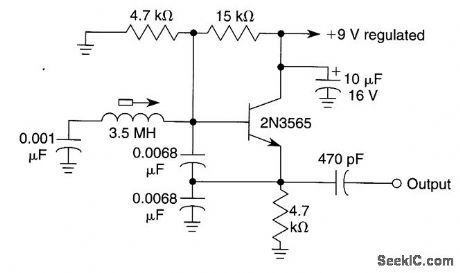
DARLINGTON_TRANSISTOR_OSCILLATOR
Published:2009/6/23 2:23:00 Author:May

This oscillator uses a very large capacitance-to-inductance ratio. L1 is a one-tum coil consisting of a loop of #12 wire 12 in diameter. This circuit is useful for metal detectors, etc., where a loop antenna is used. (View)
View full Circuit Diagram | Comments | Reading(0)
HF_VFO_CIRCUIT
Published:2009/6/23 2:22:00 Author:May

This typical HF VFO circuit has several stability-enhancing features, including well-chosen capacitor types. The frequency of the VFO is approximately 2π (C1 + C2 + C3) L1. L1 should be an aircore type coil, rigidly mounted, with high (>200 value) value of Q. (View)
View full Circuit Diagram | Comments | Reading(0)
Simple 51 test board
Published:2011/7/25 3:01:00 Author:Ecco | Keyword: Simple, 51 , test board

It can complete the water lights directly, digital dynamic static display, small speakers sing, 24c02 read and write, keyboard control, serial communications test. (View)
View full Circuit Diagram | Comments | Reading(1465)
CAPACITOR_HYSTERESIS_COMPENSATOR
Published:2009/6/23 2:22:00 Author:May

View full Circuit Diagram | Comments | Reading(0)
COMPLEMENTARY_OR_BILATERAL_ac_EMITTER_FOLLOWER_CIRCUIT
Published:2009/6/23 2:20:00 Author:May

This noninverting circuit uses a pair of com-plementary npn (2N3904) and pnp (2N3906) transistors. (View)
View full Circuit Diagram | Comments | Reading(0)
GROUNDED_BASE_TUNED_COLLECTOR_OSCILLATOR_FOR_AM_BROADCAST_BAND
Published:2009/6/23 2:20:00 Author:May

View full Circuit Diagram | Comments | Reading(0)
ELECTRONIC_FISH_LURE
Published:2009/6/23 2:56:00 Author:Jessie

The click-click sound lures fish to the vicinity, where your bait or lure can do the rest. The trans-former is a subminiature type with a 500-Q, center-tapped primary and a 3.2-Q secondary. Put the circuit in a watertight container and lower it into the water. (View)
View full Circuit Diagram | Comments | Reading(191)
VLF_LC_OSCILLATOR
Published:2009/6/23 2:19:00 Author:May

The VLF oscillator uses a large toroid coil as the frequency-determining component and a 2N5485 FET as the active device. R3 is used as a feedback control and also by running the circuit with slightly less feedback than needed for oscillation, can serve as a regenerative amplifier or detector. (View)
View full Circuit Diagram | Comments | Reading(2482)
Simple sine wave generator composed of μA741
Published:2011/7/29 2:12:00 Author:Ecco | Keyword: Simple, sine wave , generator


The chart shows a simple sine wave generator circuit. The circuit can produce the sine wave with less distortion, the oscillation frequency:
According to the data presented in this chart, the oscillation frequency is about 25Hz. Changing the value of inductor L and capacitor C can change the oscillation frequency from 15Hz to 100kHz, the total harmonic distortion can be less than 0.5%, while the upper frequency limit is controlled by the operational amplifier. The potentiometer R1 can adjust the amount of positive feedback added to series resonant circuit. Oscillation condition is that resistor R1 should be equal to the inductance sum of DC resistor RL and inductor. Diode D1 is used to limit the signal voltage to prevent saturation of inductor and operational amplifier. In order to get the distortion as small as possible, the value of resistor R1 should be as low as possible, it but must be able to ensure the maintenance of oscillation.
(View)
View full Circuit Diagram | Comments | Reading(3119)
PHOTO_SUPER_STROBE
Published:2009/6/23 2:55:00 Author:Jessie

A change in audio or light level on the sensor connected to J1 is amplified by IC1-a and IC1-b (rectified), and used to trigger IC2. R12 sets the delay between the trigger and the flash. IC1-c drives indicator LED2 and triggers SCR1, which sets off the strobe connected to J2. A photo cell or a microphone can be used as a sensor. (View)
View full Circuit Diagram | Comments | Reading(689)
| Pages:1370/2234 At 2013611362136313641365136613671368136913701371137213731374137513761377137813791380Under 20 |
Circuit Categories
power supply circuit
Amplifier Circuit
Basic Circuit
LED and Light Circuit
Sensor Circuit
Signal Processing
Electrical Equipment Circuit
Control Circuit
Remote Control Circuit
A/D-D/A Converter Circuit
Audio Circuit
Measuring and Test Circuit
Communication Circuit
Computer-Related Circuit
555 Circuit
Automotive Circuit
Repairing Circuit