
Circuit Diagram
Index 1368
74 series digital circuit of 7450, 74H50 dual 2 input and-nor gate
Published:2011/7/21 3:08:00 Author:Ecco | Keyword: digital circuit , 2 input , negater

7450, 74H50 dual 2 input and-nor gate
(View)
View full Circuit Diagram | Comments | Reading(565)
HEARTBEAT_TRANSDUCER
Published:2009/6/23 2:58:00 Author:May

A simple heart-beat transducer can be made from an infrared LED and an infrared phototran-sistor. It works because skin acts as a reflective surface for infrared light. The IR reflectivity of one's skin depends on the density of blood in it. Blood density rises and falls with the pumping action of the heart. So the intensity of infrared reflected by the skin(and thus transmitted to the phototran-sistor)rises and falls with each heartbeat. (View)
View full Circuit Diagram | Comments | Reading(2716)
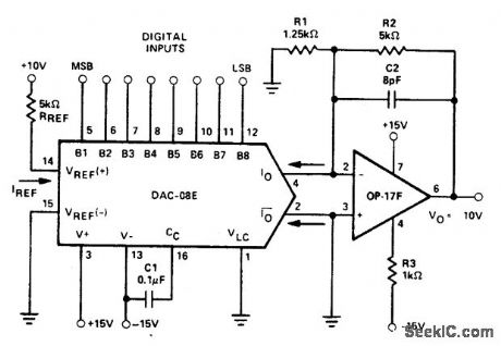
SUMMING_AMPLIFIER_WITH_LOW_INPUT_CURRENT
Published:2009/6/23 2:57:00 Author:May
View full Circuit Diagram | Comments | Reading(581)
AUDIO_MIXER
Published:2009/6/23 2:56:00 Author:May

Designed around an LM3900 quad op amp, this mixer combines 2-line and 2-mike inputs and sums them at the output terminal. R7 through R10 can be changed to vary the gain (around +23 dB). (View)
View full Circuit Diagram | Comments | Reading(0)
DELAYED_VIDEO_TRIGGER_FOR_SCOPES
Published:2009/6/23 2:49:00 Author:May

This circuit will extract vertical sync from a video signal, produce a vertical sync pulse, and add an adjustable delay. This permits a delayed sweep effect to enable a scope to look at any particular horizontal line. It is useful for older scopes. (View)
View full Circuit Diagram | Comments | Reading(905)
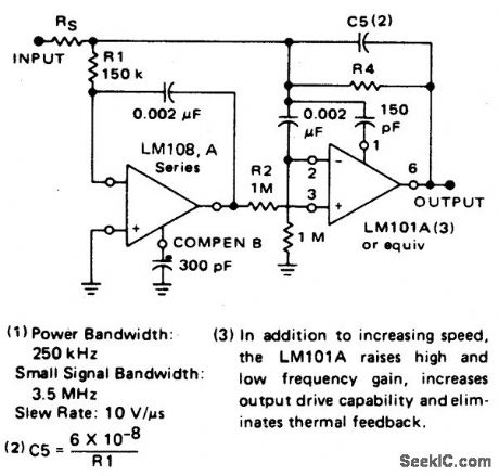
HIGH_SPEED_CURRENT_TO_VOLTAGE_OUTPUT_AMPLIFIER
Published:2009/6/23 2:48:00 Author:May
View full Circuit Diagram | Comments | Reading(492)
The open-state level test circuit diagram indicated by lighting Dp decimal point
Published:2011/7/20 20:16:00 Author:Ecco | Keyword: open-state, level test , indicated , lighting, Dp decimal point

The open-state level test circuit diagram indicated by lighting Dp decimal point is shown as the chart. VT is conducted when it is in high level, it indicates H; VT is cut off when it is in low level, pin 1 of 7402 is in high level, it indicates L; when probe opens the circuit, pin 2,3 of 7402 are input high level, pin 1 outputs low level. At the same time, VT cuts off, pin 5 is pulled down in low level by R4, only pin 4 outputs high level to drive dp decimal point to emit.
(View)
View full Circuit Diagram | Comments | Reading(773)
CURRENT_BOOSTER
Published:2009/6/23 2:48:00 Author:May

View full Circuit Diagram | Comments | Reading(523)
DIFFERENTIAL_AMPLIFIER_FOR_SCOPES
Published:2009/6/23 2:47:00 Author:May

Differential inputs and comparator modes can be added to any general-purpose oscilloscope using this circuit setup. Calibration doesn't change because the circuit operates in unity gain in most modes. Amplifier noise level is low enough not to degrade low-level signals, and its dynamic range can handle signals up to ±12V peak. Notice that all of the resistors are 1%, unless specified otherwise. (View)
View full Circuit Diagram | Comments | Reading(2939)
LOW_NOISE_4_CHANNEL_GUITAR_MIXER
Published:2009/6/23 2:47:00 Author:May


IC1-a,IC1-b,IC2-a,and IC2-b all function with a gain of about 19. Their outputs are mixed via the level-control pots and the resulting signal amplified by IC3-a and fed to tone-control stage IC3-b.Finally,the output from IC3-b is fed to unity gain buffer stage IC4-a via volume-control potgntiometer VR8. (View)
View full Circuit Diagram | Comments | Reading(1733)
CABLE_BOOTSTRAPPING
Published:2009/6/23 2:47:00 Author:May

Bootstrapping input shield for a follower reduces cable capacitance, leakage, and spurious voltages from cable flexing. Instability can be avoided with small capacitor on input. (View)
View full Circuit Diagram | Comments | Reading(684)
SIMPLE_REMOTE_GAIN_CONTROL
Published:2009/6/23 2:46:00 Author:May


The listing is a test program that demonstrates circuit operation using an IBM-compatible PC. To form a subroutine for a main program, use lines 330 to 380, deleting line 360. The calling program then would pass values for X(wiper direction)and C(number of increments). (View)
View full Circuit Diagram | Comments | Reading(535)
Benz C220 WDB H A22 EXRH 123456 identification code circuit diagram
Published:2011/7/20 20:17:00 Author:Ecco | Keyword: Benz, WDB, H , A22 , EXRH, 123456 , identification code
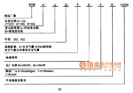
View full Circuit Diagram | Comments | Reading(402)
ROOM_MONITOR
Published:2009/6/23 3:17:00 Author:Jessie

The circuit uses Q1 to buffer the right-channel balance output while Q2 and Q3 form a VOX circuit. When the signal level from the microphone goes high, the output of the VOX also goes high and the multiplexer inside IC1 switches the high-gain left-channel output through to a following buffer stage. This signal is then ac-coupled via C3 into an RE mixer stage and thence to an RF amplifier, which is tuned by C2 and L2. (View)
View full Circuit Diagram | Comments | Reading(3094)
555_FM_CIRCUIT
Published:2009/6/23 3:12:00 Author:Jessie

Circuit for applying a dc-coupled FM or PPM to a 555 configured as an oscillator. (View)
View full Circuit Diagram | Comments | Reading(1546)
Simple dimmer circuit diagram
Published:2011/7/28 2:12:00 Author:Ecco | Keyword: Simple dimmer

Simple dimmer
Figure 12 is a simple dimmer circuit, the adjustment of light is controlled by the multi-file switch K, when K sets to 1 , the lights are off; when the K sets to 2 , the light is shinedby the capacitor connecting; when K sets to 3 , the power is supplied to the lamp through the diode half-wave rectifier, the lamp's brightness is about half of usual; when the K sets to 4 , the light bulb works in the rated voltage, the brightness is brightest.
(View)
View full Circuit Diagram | Comments | Reading(697)
FAST_VOLTAGE_FOLLOWER
Published:2009/6/23 2:44:00 Author:May
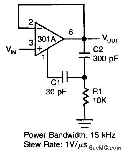
View full Circuit Diagram | Comments | Reading(588)
POWER_LINE_MODEM_FOR_COMPUTER_CONTROL
Published:2009/6/23 3:10:00 Author:Jessie

This circuit uses an 87C57 microcontroller and a few peripherals to condition X-10 power-line carrier-code formats from a personal computer to use an X-10 power-line interface in a home-control system. Software details are available in the reference. (View)
View full Circuit Diagram | Comments | Reading(3217)
SAMPLING_RATE_PHASE_LOCK
Published:2009/6/23 2:44:00 Author:May


Most digital scopes have record lengths that are power of 2 (e.g., 1024 points) and sampling rates constrained to a 1-2-5 sequence. This can lead to measurement errors on power-line waveforms because an integral number of line cycles can't be captured. Digital scopes that calculate measurements, such as the rms level, across the entire record will be in error.One solution to this problem is to phase-lock the scope's sampling rate to the line frequency by exploiting the external clock input found on some digital scopes. Phase-locking the sampling to line frequency also tracks variations in the power-line frequency.A 9- or 12-Vac wall transformer provides the circuit's power and the frequency reference. The negative output of the diode bridge refines the circuit ground. The 78L05 regulator provides the +5 V supply for the three ICs. R3 and C2 create a low-pass filter on the half-cycles from one of the floating transformer outputs. R3 also limits the current into the internal diode clamps of the inverter gate.The inverter output becomes the power-line frequency reference and is one input (SIG in to the phase comparator) of the Signetics 74HC4046A phase-locked loop (PLL). The 74HC4040 divides the PLL output frequency by 1024 and feeds the divided clock back to the other PLL phase-comparator input (COMP in). The phase-comparator output (PC2) is filtered and drives the PLL's control voltage (VCO in) so that the output frequency is 1024 times the reference frequency.With the loop filter shown, the output frequency locks to the line frequency in about 10 s. The oscillator is locked to both 50- and 60-Hz inputs using a 74HC4046A and the values shown for resis-tors RI and R2 and capacitor C1.The output signal is buffered and sent to the scope's external clock input, which is typically a TTL-compatible input. A different tap from the 74HC4040 can be selected to control the number or cycles captured in one scope record. (View)
View full Circuit Diagram | Comments | Reading(1146)
455_kHz_MODULATOR
Published:2009/6/23 3:10:00 Author:Jessie

This circuit shows how to frequency-modutate the oscillator using a 555. Oscillator frequency is set with the 5-kΩ potentiometer and the modulation signal is dc-coupled. (View)
View full Circuit Diagram | Comments | Reading(1537)
| Pages:1368/2234 At 2013611362136313641365136613671368136913701371137213731374137513761377137813791380Under 20 |
Circuit Categories
power supply circuit
Amplifier Circuit
Basic Circuit
LED and Light Circuit
Sensor Circuit
Signal Processing
Electrical Equipment Circuit
Control Circuit
Remote Control Circuit
A/D-D/A Converter Circuit
Audio Circuit
Measuring and Test Circuit
Communication Circuit
Computer-Related Circuit
555 Circuit
Automotive Circuit
Repairing Circuit