
Circuit Diagram
Index 1369
FM_MODULATOR
Published:2009/6/23 3:08:00 Author:Jessie

The FM modulator is built with a Motorola MC1648P oscillator. Two varactors, Motorola MV209, are used to frequency modulate the oscillator. The 5000-Ω potentiometer is used to bias the varactors for best linearity. The output fre-quency of approximately 100 MHz can be ad-justed by changing the value of the inductor. The output frequency can vary as much as 10 MHz on each side. The output level of the modulator is -5 dBm. In this prototype, the varactor bias was 7.5 V for best linearity; but this could be different with other varactors. (View)
View full Circuit Diagram | Comments | Reading(2565)
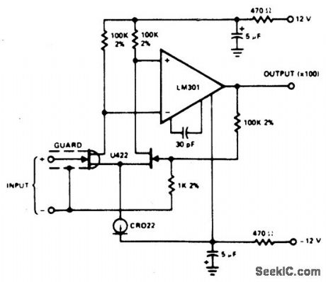
ISOLATION_AMPLIFIER_FOR_CAPACITIVE_LOADS
Published:2009/6/23 2:43:00 Author:May
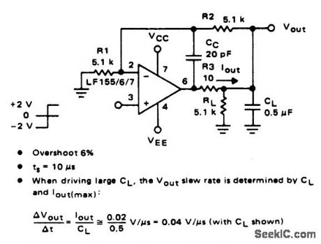
View full Circuit Diagram | Comments | Reading(506)
ac_POWER_LINE_MONITOR
Published:2009/6/23 3:07:00 Author:Jessie

When the power-line voltage source fails,Q1 turns on,activates optoisolator U2, and triggers SCR1.For small SCRs,U1 might directly trigger SCR1. (View)
View full Circuit Diagram | Comments | Reading(1317)
MUTING_CIRCUIT
Published:2009/6/23 2:43:00 Author:May

The circuit operates as follows: The signal is input to Vin and a dc control voltage is applied to VC. Vbias determines the desired bias point current. Assuming the following component and voltage values:
VCC=7.6 VdcVbias=1 VdcVin=1Vp-p,ac signal centered about 3.8 Vdc biasRL=2kΩRE=200kΩRE1=2kΩ
Q3 bias current is 1 mA, and dc output voltage is about 5.8Vwith an ac gain of about -1, Q1 and Q2 form a current switch and Q3 acts as a constant current source.For unmuted operation, Vc=0Vdc, and all of the bias current flows through Q1. Consequently, the circuit operates as a normal common emitter stage, with ac gain=-RL/RE1,. When Vc=5Vdc, all of the bias current flows through Q2, reducing the signal gain to zero. However, because the same dc current flows through RL, in both cases(unmuted and muted), the bias point at the output remains fixed. The Cc/RE1network is required to bypass the Q3 current source(which is a high impedance)to achieve alow ac impedance at the emitter of the Q1 common emitter stage during unmuted oper-ation. Cc is chosen to be a short circuit at signal frequencies of interest. The circuit works best if the Q1 and Q2 pair is matched. Typical change in the output dc voltage from unmuted to muted condi-tion is <5 mVdc.
RL,RE, and Vbias are chosen for desired dc operating conditions and signal dynamic range. Vbias, can be generated via a VCC voltage divider. The signal at Vin, can be ac coupled, but a bias circuit must be added to Q1's base to generate a dc component. RE1 is chosen for desired ac gain. Vin must be cen-tered about a dc component, and, to assure proper switching action, VCTRL, must be higher than Vin, by an amount greater than one VBE drop. (View)
View full Circuit Diagram | Comments | Reading(679)
WIDE_BANDWIDTH_LOW_NOISE_LOW_DRIFT_AMPLIDIER
Published:2009/6/23 3:06:00 Author:Jessie
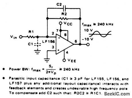
View full Circuit Diagram | Comments | Reading(537)
INRUSH_CURRENT_LIMITER
Published:2009/6/23 2:40:00 Author:May

A 7805 can be configured as a constant-current regulator, to serve as an inrush current limiter. R1 will have 5V across it at all times so the total current through I1 will be 5 V/R1 + 5 mA, the 5 mA being the regulator operating current. In this case, R1 = 5 V/95 mA = 52.6Ω for I1 current = 100 mA. (View)
View full Circuit Diagram | Comments | Reading(0)
DC_TO_VIDEO_LOG_AMPLIFIER
Published:2009/6/23 3:05:00 Author:Jessie
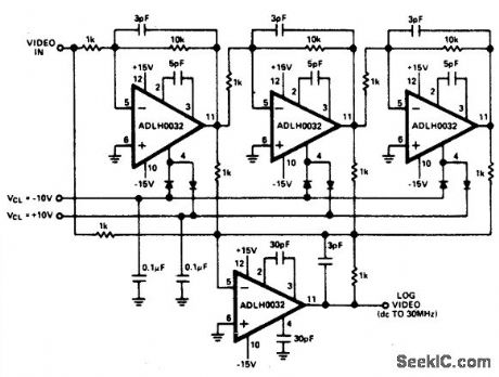
View full Circuit Diagram | Comments | Reading(434)
±100_V_COMMON_MODE_RANGE_DIFFERENTIAL_AMPLIFIER
Published:2009/6/23 3:04:00 Author:Jessie
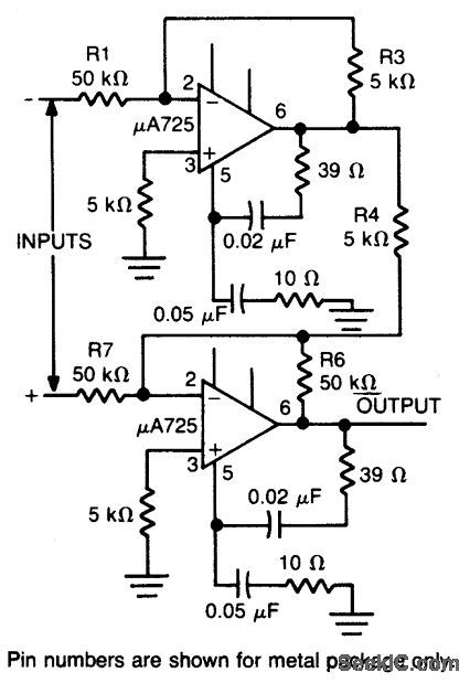
View full Circuit Diagram | Comments | Reading(413)
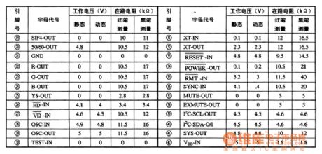
The internal block circuit diagram of LA7680 IC
Published:2011/6/23 2:45:00 Author:Ecco | Keyword: internal block , IC

LA7680 is a small TV signal processing monolithic integrated circuit which is produced by Sanyo company of Japan. It is widely used in various types of domestic and imported large screen color TV. The featuresand functionsLA7680 IC contains images and audio amplifier circuit, color demodulation circuit, the luminance signal processing circuit, line scanning and field scanning small signal processing circuit, voltage controlled oscillator circuit, PAL / NTSC standard switch circuit, sync separator circuit and AFT control circuit. The IC's internal circuit block diagram is shown as the chart.
The internal block circuit diagram of LA7680 IC is shown as the chart. (View)
View full Circuit Diagram | Comments | Reading(4701)
ac_POWER_CONTROLLER
Published:2009/6/23 3:04:00 Author:Jessie

This circuit is used to vary the power delivered to a 120-Vac load under software control. A 68705 micro controller can control eight discrete power triacs, each of which delivers power in 82 smoothly graduated steps, ranging from 0 to 97% of full power. The value delivered to one channel is independent of the value delivered to any other channel. Loads can include light displays, universal motors, heaters, and other appliances.The power level is set by software, not a potentiometer. The software includes a basic set of routines for processing interrupts and setting the power level. The software also includes five test and demonqtration routines for putting the circuit through its paces. Moreover, there's plenty of room to add your own routines to the 68705's built-in EPROM.The basic circuit is simple, yet versatile enough to accept inputs from on-board DIP switches; al-ternatively, the inputs can be driven from a microcomputer bus or parallel port, or a stand-alone device with TTL-compatible outputs. There are 12 input bits to set modes and specify values. (View)
View full Circuit Diagram | Comments | Reading(1940)
ULTRA_LOW_LEAKAGE_PREAMP
Published:2009/6/23 3:03:00 Author:Jessie
Input leakage-2 pA at 75℃. (View)
View full Circuit Diagram | Comments | Reading(470)
TMP87CH36 monolithic microcomputer integrated circuit diagram
Published:2011/7/25 3:00:00 Author:Ecco | Keyword: monolithic , microcomputer , integrated circuit
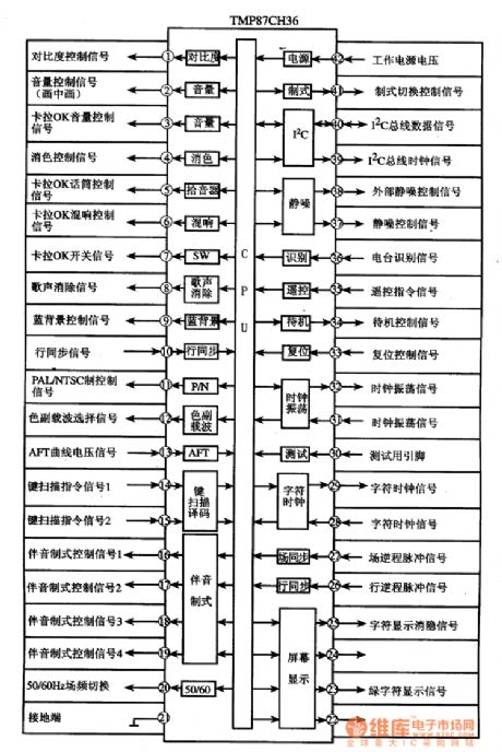
TMP87CH36 is the single-chip microcomputer integrated circuit produced by Toshiba, andit is widely used in Changhong, Toshiba series of movement and large-screen color TV. 1. Featuresand functionsTMP87CH36 integrated circuits is mainly composed of the central processing (CPU), I2C bus control circuit, key scan decoding circuit, the character display circuit, mode control circuit, frequency control circuit, to be ideological power control circuit, squelch control circuit, the clock oscillation circuit, the characters display the clock circuit, 5W6OHz field frequency switching circuit, the volume and contrast control circuit, and other auxiliary functions circuit.2. Pin functions and data TMP87CH36 integrated circuit uses the plastic package with 42 feet in double rows, the pin functions and signal flowing are shown in Figure 1, the pin letter code and data are listed in Table 1.
(View)
View full Circuit Diagram | Comments | Reading(533)
SCOPE_VOLTAGE_CURSOR_ADAPTER
Published:2009/6/23 2:39:00 Author:May

The voltage cursor adapter superimposes horizontal cursor lines on the top and bottom of the waveform-a kind of electronic calipers-to perrrtit direct readout of the voltage value. The cursor lines extend across the entire screen. The MC78L12 voltage regulator (IC1) supplies regulated 12 Vdc to the rest ofthe circuit. The ICM7555 timer (IC2) drives the CD4066B, a CMOS bilateral switch (IC3). This drive frequency can either be a normal frequency (NORM) of 100 Hz or a low-frequency (LO-F) of 10 kHz, depending on the setting of switch S1. Set S1 to LO-F for inputs below 500 Hz.The dc reference voltage supplied to pin 3 of IC3 is set by R3, a 10-turn, 5000-Ω precision potentiometen The voltage can be read directly from a turns counter dial coupled directly to the potentiometer's wiper. The accuracy of this reading can be 1% or better. Trimmer potentiometer R1 permits the voltage to R3 to be calibrated to precisely 10 V.The circuit is calibrated by setting the digital reading on the turns counter of R3 to the full clockwise position and adjusting R1 for a reading of 10 V at the wiper of R3 with a digital voltmeter.Bilateral switch IC3 converts the dc reference to a square wave with exactly the same wiper amplitude. The square-wave output appears on common pins 4, 9, and 10 of IC3 and coaxial plug PL1. (View)
View full Circuit Diagram | Comments | Reading(934)
NE6O2_dc_POWER_CIRCUITS
Published:2009/6/23 2:38:00 Author:May

The dc power supply circuit for the NE-602. (View)
View full Circuit Diagram | Comments | Reading(565)
AMPLIFIER_COOL_DOWN_CIRCUIT_II
Published:2009/6/23 2:37:00 Author:May
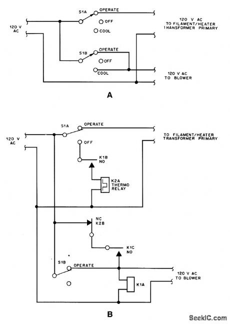
High-power amplifiers used In RE service,usmg vacuum tubes,often benefit from leaving the blower air flow on after removal of filament/heater voltage. (View)
View full Circuit Diagram | Comments | Reading(502)
The flashing switch circuit controlled by light intensity(the lamp shining in the speed of 1.5KHZ)
Published:2011/7/28 2:14:00 Author:Ecco | Keyword: flashing switch , light intensity, 1.5KHZ

In the light degree of 13 ~ 25lx, the lamp flashes in the frequency of 1.5Hz. The circuits work as a multivibrator. When the light intensity is over 25lx, the value of photosensitive resistor is low, transistor T2 turns on, lights off. The diode BA127stops the transistor T1.
In order to make the multivibrator work in low illumination, it needs to connect a spinner resistor to thephotosensitive resistor in parallel to limit the increasingrate of theresistance of photosensitive.
The main technical data:
UB=4V, the light intensity is 45lx, it turns off;
UB=5V, the light intensity is 25lx, it turns off;
UB=6V, the light intensity is 15lx, it turns off;
The voltage of the lamp: 2~4V
The current consumption(100lx): <10mA
The environment temperature: -10~+50℃ (View)
View full Circuit Diagram | Comments | Reading(590)
HARTLEY_OSCILLATOR
Published:2009/6/23 2:35:00 Author:May
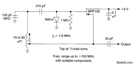
This circuit uses a tapped inductor in a Hartley oscillator circuit. The tap is generally at 25 to 35% total tums in most instances. (View)
View full Circuit Diagram | Comments | Reading(925)
SIMPLE_SCHMITT_TRIGGER
Published:2009/6/23 2:34:00 Author:May
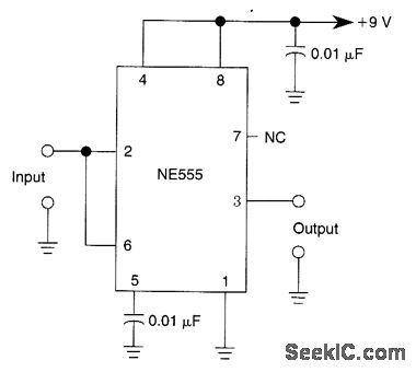
A 555 IC is shown configured to function as a Schmitt trigger. Inputs above and below the threshold level will turn the circuit on and off producing a square wave output. (View)
View full Circuit Diagram | Comments | Reading(759)
TV_HORIZONTAL_DEFLECTION_CIRCUIT
Published:2009/6/23 2:34:00 Author:May

The circuit illustrates the method of using two SCR devices in a TV horizontal deflection application. This circuit was widely used by certain TV manufacturers as an alternate to the vacuum tube or transistor deflection circuit. (View)
View full Circuit Diagram | Comments | Reading(3302)
TUNED_COLLECTOR_OSCILLATOR
Published:2009/6/23 2:34:00 Author:May
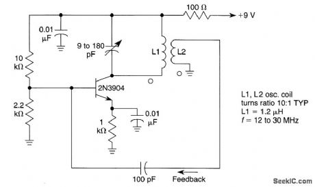
View full Circuit Diagram | Comments | Reading(926)
| Pages:1369/2234 At 2013611362136313641365136613671368136913701371137213731374137513761377137813791380Under 20 |
Circuit Categories
power supply circuit
Amplifier Circuit
Basic Circuit
LED and Light Circuit
Sensor Circuit
Signal Processing
Electrical Equipment Circuit
Control Circuit
Remote Control Circuit
A/D-D/A Converter Circuit
Audio Circuit
Measuring and Test Circuit
Communication Circuit
Computer-Related Circuit
555 Circuit
Automotive Circuit
Repairing Circuit