
Circuit Diagram
Index 1365
Electronic hypnotic device 3
Published:2011/7/29 3:01:00 Author:Ecco | Keyword: Electronic, hypnotic device

This example describes a simple electronic hypnosis device circuit, it has less circuit components,and it iseasy to make.
The working principle.
The electronic hypnosiscircuit is non-steady-state multi-harmonic oscillator circuit which is composed ofthe time base ICand relatedexternal components, it is shown in Figure 9-140.
After turning on power switch S, +6 V voltage is applied to 4 feet and 8 feet of IC to provide power supply for the IC. After multivibrator oscillation, the pin 3 of IC outputs low-frequency oscillation pulse signal, and it is combined by the capacitor C2 and added to the speaker BL, then it issues the simulated sound of dripping water. The voice has hypnotic effects for insomnia. Adjusting potentiometer RP can change capacitor Cl and the operating frequency of multivibrator. The selection of componentsR selects 1/4W carbon film resistor. RP uses small solid potentiometer or sealed variable resistor. Cl and C2 select the electrolytic capacitor with voltage in lOV. IC uses NE555 or μA555, LM555, 5G1555, FX555 and other models of time-base integrated circuits.
(View)
View full Circuit Diagram | Comments | Reading(3230)
Electronic hypnotic device 4
Published:2011/7/29 2:43:00 Author:Ecco | Keyword: Electronic , hypnotic device

The electronic hypnotic device described in the example can generate simulated sound of dripping water and be used for the treatment for insomnia.
The working principle.
The electronic hypnotic deviceis composed of the oscillator circuit, boost charging circuit and the rain sound formation circuit, it is shown in Figure 9-141.
Oscillator circuitis composed of the battery GB, control button S, transistor V, potentiometer RP, resistor Rl and Wl, W2 windings of oscillation transformer T.
Boost charging circuitis composed of the W3 winding of T, rectifier diode VD and capacitor C.
The sound of raindrops forming circuit is composed of resistors R2-R5, neon lights HLl-H4 and buzzer HAl-HA4.
R1-R5 select 1/4W metal film resistors.
RP uses multi-turn wirewound potentiometers.
C usesaluminium electrolytic capacitor with the voltage in 400V, the leakage is aslowas possible.
VD selects lA, l0OOV rectifier diode.
V uses 3AX31 germanium PNP transistor.
HAl-HA4 use HTD-27A piezoelectric buzzer with help tune. (View)
View full Circuit Diagram | Comments | Reading(1042)
BABY_MONITOR
Published:2009/6/23 3:31:00 Author:May

Transmitter operation. Operating power for the transmitter circuit is derived directly from the ac line. The dc power to operate the circuit is generated in two stages, one for an RE power-amplifier stage, and the second for the remainder of the circuit.
The ac line voltage is applied to D1 , which half-wave rectifies the ac input . The resulting dc voltage (approximately 30V under load) is fed across an RC filter (comprised of R1 and C1) and used to operate amplifier, Q1. The second stage of the power supply (composed of LED1, R2, D2, D3, C2, and C3, which forms a regulated +13.6-V, center-tapped supply) feeds the remainder of the circuit. LED1 is connected in series with R2 and is used as a visual power-on indicator for the transmitter.
An electret microphone element (MIC1) is used as the pick-up. The output of the microphone is ac coupled through C5 to UI-a (a noninverting op amp with a gain of about 100). The output of U1-a at pin 1 is ac coupled through C4 to the noninverting input of UI-b (which provides an additional gain of 48) at pin 5. The output of UI-b at pin 7 is then fed through D4 and RIO, and across R11 and C6 to the inverting input of UI-c which is biased to a positive voltage that is set by SENSITIVITY-control R19. This represents a threshold voltage at which the output of UI-c switches from high to low.
During standby, the output of UI-c at pin 8 is held at about 12 V when the voltage developed across C6 is less than the bias-voltage setting at pin 10. When a sound of sufficient intensity and du-ration is detected, the voltage at pin 9 of UI-c exceeds the threshold level (set by R19), causing UI-c's output at pin 8 at go low. That low is applied to pin 2 of U2 (a 555 oscillator/timer configured as a monostable multivibrator). This causes the output of U2 to go high for about one second, as de-termined by the time constant of R12 and C7. The output of U2 at pin 3 is applied to pin 4 of U3 (a second 555 oscillator/timer that is conftgured for astable operation, with a frequency of about 125 kHz). That causes U3 to oscillate, producing a near square-wave output that is used to drive Q1 into conduction. The output of Q1 is applied across a parallel-tuned circuit composed a T1's primary and C8. The tuned circuit, in turn, reshapes the 125-kHz signal, causing a sine-wave-like signal to appear across both the primary and the secondary of Tl.
The signal appearing at T1's secondary (about 1 or 2 V peak-to-peak) is impressed across the ac power line, and is then distributed throughout the building without affecting other electrical appli-ances connected to the line. Transient suppressor D7 is included in the circuit to help protect Q1 from voltage spikes that might appear across the power line and be coupled to the circuit through T1.
Receiver operation. Power for the receiver, as with the transmitter, is derived from a tradi-tional half-wave rectifier (D5). The resulting dc voltage is regulated to 27 V by D6 and R20, and is then filtered by C11 to provide a relatively clean, dc power source for the circuit. A light-emitting diode, LED2, connected in sGries with R20 provides a visual indication that the circuit is powered and ready to receive a signal.
The 125-kHz signal is plucked from the ac line and coupled through R21 and C12 to a parallel-tuned LO circuit, consisting of C13 and L1. That LO circuit passes 125-kHz signals while attenuating all others. The 125-kHz signal is fed through C14 to the base of Q2 (which is configured as a high-gain linear amplifier), which boosts the relatively low amplitude of the 125-kHz signal. The RE out-put of Q2 is ac coupled to the base of Q3 through C15. Transistor Q3 acts as both an amplifier and detector. Because there is no bias voltage applied to the base of Q3, it remains cut off until driven by the amplified 125-kHz signal. When Q3 is forward biased, its collector voltage rises.
Capacitor C16, connected across Q3's collector resistor, filters the 125-kHz signal so that it is essentially dc. When the voltage at the collector of Q3 rises, Q4 is driven into conduction. That causes current to flow into piezo buzzer BZ1, producing a distinctive audio tone that alerts anyone within earshot that the baby needs attention. (View)
View full Circuit Diagram | Comments | Reading(0)
MASTER_SLAVE_DEVICE_ERROR_CHECKER
Published:2009/6/23 3:30:00 Author:May

An error-check mechanism introduced into master and slave communication devices can indi-cate mismatches when both the master and slave start sending data simultaneously. The error ftag goes high and indicates a mismatch in the data.The master is the one that can interrupt the communication from a device at the other end and force it to listen. It does this forcing a low voltage level over the communication line by raising the control line to a high level. This inhibits data flow over the tines from the slave device. As a result, the slave turns into a listen mode(not a hardware feature, but rather incorporated in the software). The slave device can transmit the data after communication from the master device ceases. (View)
View full Circuit Diagram | Comments | Reading(0)
NE6O2_POWER_SUPPLY_OPTIONS
Published:2009/6/23 4:00:00 Author:Jessie

Here, Figs. 68-11A through 68-11C show an RC-filter used as both current limiter (R1) and integrator (C1), as well as for isolation. In Fig. 68-11A, +4.5 to 8.0 Vdc is the normal operating range of the NE602. In Fig. 68-11B, R1 drops voltage, and is used because a +9-V battery can go higher, and a +9-Vwall supply can produce up to 11 V. In Fig. 68-11C, a +8- to 18-Vdc supply is regulated using a 8.2-V Zener for D1. (View)
View full Circuit Diagram | Comments | Reading(480)
33_V_SWITCHING_REGULATOR
Published:2009/6/23 3:59:00 Author:Jessie


For the LT1129-3.3, dissipation amounts to a little under 1.5 W at full output current. The 5-lead surface-mount DD package handles this without the aid of a heatsink, provided that the device is mounted over at least 2500 mm2 of ground or power-supply plane. Efficiency is around 62%; dissi-pation in linear regulators becomes prohibitive at higher current levels, where they are supplanted by high-efficiency switching regulators. The synchronous buck converter is implemented with an LTC1148-3.3 converter. The LTC1148 uses both Burst ModeTM operation and continuous, constant off-time control to regulate the output voltage, and maintain high efficiency across a wide range of output loading conditions. (View)
View full Circuit Diagram | Comments | Reading(1925)
VIDEO_MASTER
Published:2009/6/23 3:58:00 Author:Jessie

The video master consists of a series of converters that place all your video sources on unused UHF channels, which then combines them with normal TV channels (terrestrial or cable into one ca-ble). That one cable can then feed several TV sets for whole-house coverage. The desired video source is selected with the TV set's tuner. All of the TV's remote-control features are retained.A complete kit of parts is available from North Country Radio, P.O. Box 53, Wykagyl Station, New Rochelle, NY 10804-0053A. (View)
View full Circuit Diagram | Comments | Reading(1215)
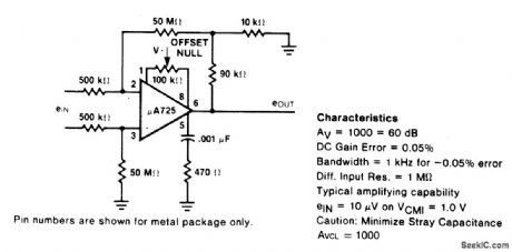
HIGH_IMPEDANCE,HIGH_GAIN,HIGH_FREQUENCY_INVERTING_AMP
Published:2009/6/23 3:29:00 Author:May
View full Circuit Diagram | Comments | Reading(459)
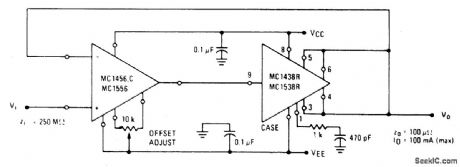
NONINVERTING_AMPLIFIER
Published:2009/6/23 3:28:00 Author:May
View full Circuit Diagram | Comments | Reading(1101)
1IC_REGULATOR_PROTECTION
Published:2009/6/23 3:56:00 Author:Jessie

This circuit protects an IC regulator against various fault conditions. (View)
View full Circuit Diagram | Comments | Reading(1816)
PREAMPLIFIER_AND_HIGH_TO_LOW_IMPEDANCE_CONVERTER
Published:2009/6/23 3:28:00 Author:May
This circuit matches the very high impedance of ceramic cartridges, unity gain, and low impedance output. By loading the cartridge with a 2M2 input resistance, the cartridge characteristics are such as to quite closely compensate for the RIAA recording curve. The output from this,preamp may be fed to a level pot for mixing. (View)
View full Circuit Diagram | Comments | Reading(2097)
JACOB’s_LADDER
Published:2009/6/23 3:28:00 Author:May

A“Iacobs Ladder”can be made from an old neon sign or oil burner ignition transformer. A rating of 12 to 15 kV at 20 to 30 mA will be adequate. Make sure to mount the electrodes to a pair of in-sulators, at least 2 apart, and bent and spaced, as shown. The ladder should be enclosed in a clear plastic housing to prevent accidental contact with the high voltage and to ensure a stable arc. Vent holes should be placed top and bottom to allow gases to escape. (View)
View full Circuit Diagram | Comments | Reading(2542)
MOISTURE_DETECTOR
Published:2009/6/23 3:55:00 Author:Jessie

The moisture detector uses two transistors and a piezoelectric transducer to sound an alarm tone when water is present. Transistor Q1 forms a crystal-controlled oscillator, using a portion of piezoelectric transducer XDC-which contains two piezoelectric crystal regions-as the crystal. The transducer has three separate leads, One lead goes to each of the crystals, and the third lead is com-rnon to both.
The smaller internal crystal region sets the frequency of operation and the larger element is driven by Q1 (when it is biased on ) to provide the loud tone output. To turn the pnp transistor Q1 (used as an oscillator) on pnp transistor Q2 (used here as a switch) must be on. To turn it on with the biasing that is normally connected, you would only need to connect a resistor from the collector of Q2 to the base, which gives the base a negative (-) bias. The resistor used is the water that is to be detected. That turns Q2 on, which, in turn, turns on Q1. The result when water touches the probe is that the transducer emits a loud sound. (View)
View full Circuit Diagram | Comments | Reading(1)
PRECISION_AMPLIFIER
Published:2009/6/23 3:26:00 Author:May
View full Circuit Diagram | Comments | Reading(409)
CURRENT_LIMITING_REGULATOR_CIRCUIT
Published:2009/6/23 3:25:00 Author:May


This regulator uses the drop across R2 to turn on Q2, removing base drive from Q1 and reducing the current through R1. About 0.65 V must be dropped across R2 before limiting occurs. To set limit current, (View)
View full Circuit Diagram | Comments | Reading(1043)
TRANSFORMERLESS_dc_POWER_SUPPLY_I
Published:2009/6/23 3:33:00 Author:Jessie

An SCR fires on the positive half cycles of the ac Iine voltage. Switched capacitors are used to select the output voltage. These must all be ac-rated, nonpolarized types. (View)
View full Circuit Diagram | Comments | Reading(711)
GROUND_LOOP_PREVENTER
Published:2009/6/23 3:32:00 Author:Jessie

Ground loops are caused by improper grounding. Ground-loop voltages can interfere with test rrteasurements because the voltages in a ground loop can be larger than the signals you're trying to measure. To prevent ground loops, use two wire plugs to provide the line power to the test instru-ments and a separate wire to bring the input grounds of the instruments to a common ground. (View)
View full Circuit Diagram | Comments | Reading(1101)
About TLC5941 Dynamic Scanning Drive Circuit
Published:2011/7/23 8:12:00 Author:Michel | Keyword: Dynamic Scanning, Drive Circuit

Here we introduce 640 x 480 full-color display system driving part design.The whole screen is composed of 4 subscreens and every subscreen manages 640 x 120 pixel range and they have single driving circuit.Because it is inner screen ,the driving design adopts dynamic scanning driving way.Drive circuit control is realized by programmable logic devices EPM1270 (Altera).
In order to improve the frame frequency, serial data uses 15 groups parallel output and every group refreshes 640 x 120 pixel range.The figure 1 shows the subscreen's single circuit.
(View)
View full Circuit Diagram | Comments | Reading(480)
SWITCHING_POWER_SUPPLY
Published:2009/6/23 3:31:00 Author:Jessie


In many switching-regulator applications for portable computers, the microprocessor is located some distance from the power supply. With the latest processors, total load currents range into several amperes. Thus, regulation at the load can become a problem.The ITH pin (pin 6) of the LTC1148 is approximately proportional to the load current. It scales nearly linearly from 0 V at no load to 2.0 V at current limit. U2, acting as a unity-gain differential amplifier, inverts the U1 pin 6 voltage (referenced to SENSE—, pin 7) and causes a current proportional to load current to flow in resistors R5 and R6. A small voltage drop appears across current-sense filter resistors R3 and R4. This' makes the voltage measured by the internal feedback divider appear low. The duty factor is adjusted to bring this back to the correct voltage. As a result, the output is increased slightly as a function of load. Capacitor C9 rolls off the high-frequency gain of the correction amplifier. (View)
View full Circuit Diagram | Comments | Reading(1008)
HIGH_INPUT_IMPEDANCE_HIGH_OUTPUT_CURRENT_VOLTAGE_FOLLOWER
Published:2009/6/23 3:25:00 Author:May
View full Circuit Diagram | Comments | Reading(650)
| Pages:1365/2234 At 2013611362136313641365136613671368136913701371137213731374137513761377137813791380Under 20 |
Circuit Categories
power supply circuit
Amplifier Circuit
Basic Circuit
LED and Light Circuit
Sensor Circuit
Signal Processing
Electrical Equipment Circuit
Control Circuit
Remote Control Circuit
A/D-D/A Converter Circuit
Audio Circuit
Measuring and Test Circuit
Communication Circuit
Computer-Related Circuit
555 Circuit
Automotive Circuit
Repairing Circuit