
Circuit Diagram
Index 1362
WAILING_SOUND_GENERATOR
Published:2009/6/23 4:45:00 Author:Jessie

In this circuit, C2 and T1 determine the tone generated and C1/R1 control the blocking rate. The signal produced is an interrupted tone, like a police whistle or toy ray gun, depending on C1 and C2. (View)
View full Circuit Diagram | Comments | Reading(600)
SCR_SWITCHING_SUPPLY_FOR_COLOR_TV_RECEIVERS
Published:2009/6/23 4:09:00 Author:May

An output +80Vat up to 1.5A is available from this supply. Aminimum load of 200 mA is required because of the SCR hold-ing current. Notice that no ac line isolation is provided and a shock hazard exists. (View)
View full Circuit Diagram | Comments | Reading(596)
POWER_EFFICIENT_VOLTAGE_REGULATOR
Published:2009/6/23 4:06:00 Author:May

Included in the many features of this power-efficient, voltage-regulator circuit is shutdown power control with a current output up to several hundred milliamperes (expandable to amperes, if desired). Current limiting can be preset to a fixed level for controlled dissipation in Q1 and the circuit requires no auxiliary voltage supply for the pass transistor. (View)
View full Circuit Diagram | Comments | Reading(663)
TRACKING_POWER_SUPPLY
Published:2009/6/23 4:03:00 Author:May

Two op amps are used in this basic op-amp regulator circuit. The outputs can be fed to current amplifier stages or emitter followers, if needed. (View)
View full Circuit Diagram | Comments | Reading(890)
The gas overranging alarm miner lamp 2
Published:2011/7/29 2:58:00 Author:Ecco | Keyword: gas overranging, alarm, miners lamp

The gas overranging alarm miner lamp described in the example is based on miner's lamp or miner's helmet. It couldflash in time to remind miners paying attention on safety.
The working principle: The gas overranging alarm miner lamp circuit is composed of gasdetection circuit, controlled oscillator circuit and lighting circuit. It's shown as the figure 8-30.
The gas detection circuit is composed of gas sensor, resistors Rl and potentiometer RP. The controlled oscillator circuit is composed of the potentiometer RP, a diode VD, transistors Vl-V3, resistor R2 and R3, capacitor Cl and C2 and the relay K. The lighting circuit is composed of the battery GB, lights EL, the constant moving contact of S and K light switch. The switch S turns off, EL will be lit. The end of the gas sensor detects methane gas, the place between A and B shows the state with high resistance, VD and V3 are in the OFF state, K is not action, miner working in the lighting condition.
(View)
View full Circuit Diagram | Comments | Reading(679)
VIDEO_AMPLIFIER
Published:2009/6/23 4:03:00 Author:May

View full Circuit Diagram | Comments | Reading(1511)
SIMPLE_9_V_SUPPLY
Published:2009/6/23 4:02:00 Author:May

This circuit uses an LM7805 with a resistive voltage divider in the common leg of the regulator.The regulator can be fooled into producing an apparent higher output voltage in this manner. This supply is useful for running radios, tape recorders, or other 9-V devices. (View)
View full Circuit Diagram | Comments | Reading(1075)
ELECTRONIC_SIREN
Published:2009/6/23 4:44:00 Author:Jessie

In this circuit, the LM3909 is used in a simple electronic siren. When S1 is closed, C2 begins to charge rapidly through RI. When the charge on C2 reaches about 1 V, the oscillator starts. As the voltage across C1 increases toward +7, the oscillator's output frequency also increases. Releasing (opening) S1 removes power from the circuit. The oscillator continues to operate, with a decline in output volurrte and frequency until C1 discharges to about the l-V level.Experiment with the siren circuit by selecting different R1/C2 combinations to obtain a desired rise and fall output. Change the value of C1 to vary the oscillator's frequency. Keep the value of R2 at or above 47Ω to protect the IC from drawing too much current. (View)
View full Circuit Diagram | Comments | Reading(0)
SIMPLE_VIDEO_LINE_BAR_GENERATOR
Published:2009/6/23 4:02:00 Author:May
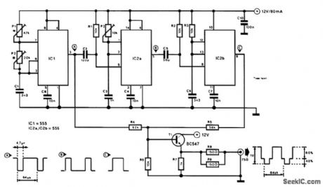
A 555 and a dual 556 timer generate a rudimentary video signal, as shown in the schematic. The first timer generates 4.7-μs synch pulses operating in the astable mode with a 64-μs period. The sec-ond timer generates a delay pulse, which triggers the third timer to generate a bar. The second timer sets the bar position and the third sets the bar width. (View)
View full Circuit Diagram | Comments | Reading(2212)
5_Vdc_REGULATED_SUPPLY
Published:2009/6/23 4:44:00 Author:Jessie

View full Circuit Diagram | Comments | Reading(832)
+5_V_AT_1_A_SUPPLY_WITH+3_TO+5_V_INPUT
Published:2009/6/23 4:43:00 Author:Jessie

A MAX741U switching-mode power-supply controller and a switching FET Q1 are used to provide +5 V at 1 A. (View)
View full Circuit Diagram | Comments | Reading(645)
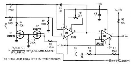
10_Hz_TO_10_kHz_3_DECADE_VCO
Published:2009/6/23 4:37:00 Author:May
View full Circuit Diagram | Comments | Reading(0)
VARACTORLESS_HF_MODULATOR
Published:2009/6/23 4:36:00 Author:May

Traditionally, high-frequency oscillators are frequency-modulated by using a varactor. However, varactors usually require a large voltage change to achieve a reasonable capacitance change-a prob-lem in many battery-powered systems.Such a problem can be overcome by employing base-charging capacitance modulation. Resistor RI establishes Q1's current, and R2 allows control of the collector bias current byVmod The trans-mission line (T1) in the negative resistance-type oscillator determines the frequency of oscillation. T1 is a high-quality, low-loss, ceramic coaxial shorted quarter-wave transmission line. Under proper terminal impedances, a negative resistance is seen at Q1's base. T1 reacts with this negative resis-tance to produce sustained oscillations.Frequency modulation is accomplished by changing Q1's collector bias current and thus chang-ing Q1's base-charging capacitance. This effect is seen at Q1's base and causes a frequency shift in the resonators quarter-wave node. (View)
View full Circuit Diagram | Comments | Reading(0)
The gas overranging alarm miner lamp 3
Published:2011/7/29 2:59:00 Author:Ecco | Keyword: gas overranging , alarm, miners lamp

The gas overranging alarm miner lamp described in the example uses the batteries of miner's lamp as power supply. It is installed in the mine cap.When the gas is over the limit, the alarm signal will remind miners to evacuate in time.
The working principle: The gas overranging alarm miner lamp circuit is composed of gas detection circuit,electronic switching circuit and sound alarm circuit. It's shown as the figure 8-31.
The gas detection circuit is composed of resistor Rl, and the gas sensor, potentiometer RP.
The electronic switching circuit is composed of thyristor VT and RP.
Thesound alarm circuit is composed of sound IC, resistor R2, transistor Vand speaker BL.
When the gas concentration is below the limit of safety standards, the conductivity between a and b of gas sensor is low, b point is in low level, VT is in the cut-off state, and IC does not work, BL does not sound.
When the gas concentration is over the limit of safety standards, the conductivity between a and b of gas sensor will increase, the voltage of b point increases, VT turns on by trigger, and IC works, the audio output signal amplified by the V will drive the alarm BL.
(View)
View full Circuit Diagram | Comments | Reading(539)
SAWTOOTH_GENERATOR
Published:2009/6/23 4:35:00 Author:May

A sawtooth waveform generator circuit using a 555 IC is shown. The IC is connected in an astable oscillator circuit with the majority of the output contained in the positive portion of the cy-cle. The negative output is a very brief pulse.Capacitor C2 charges through R3 in a positive direction during the time that the IC's output (at pin 3) is high. When the output goes negative, C2 is rapidly discharged through Dl and the IC's out-put.Peak-to-peak sawtooth output is about 1 V. The linearity of this circuit is best when R3 is as large as possible. The oscillator's frequency is about 200 Hz and can be increased by lowering either the value of R1 or C1 to decrease the frequency, increase the values of those components. (View)
View full Circuit Diagram | Comments | Reading(0)
SIMPLE_9_V_POWER_SUPPLY
Published:2009/6/23 4:42:00 Author:Jessie

This supply will provide 9-V transistor radios or cassettes from a 12-V auto electrical system. (View)
View full Circuit Diagram | Comments | Reading(700)
OP_AMP_LINEAR_SAWTOOTH_GENERATOR
Published:2009/6/23 4:34:00 Author:May

Q1 is connected in a simple constant-current generator circuit. The value of Q1's emitter resistor sets the constant-current level flowing from the transistor's collector to the charging capacitor, C1.One op amp of an LM324.quad op-amp IC, UI-a, is connected in a voltage-follower circuit. The input impedance on the voltage follower is very high and offers little or no load on the charging cir-cuit. The follower's output is connected to the input of UI-b, which is configured as a voltage com-parator. The comparator's other input is tied to a voltage-divider setting the input level to about 8 V.The output of UI-b at pin 7 switches high when the voltage at its positive input, pin 5, goes above 8 V. That turns on Q2, discharging C1. The sawtooth cycle is repeated over and over as long as power is applied to the circuit.The sawtooth's frequency is determined by the value of C1 and the charging current supplied to that capacitor. As the charging current increases, the frequency also increases, andvice versa, To in-crease the generator's frequency range, decrease the value of C1, and to lower the frequency, in-crease the value of C1. The output is about 3 to5V. (View)
View full Circuit Diagram | Comments | Reading(0)
WARBLE_OSCILLATOR
Published:2009/6/23 4:41:00 Author:Jessie

Sections A & B form an oscillator running at 2 Hz, which gates sections C and D, a 1-kHz oscilla-tor. This drives the TIP31 speaker driver. (View)
View full Circuit Diagram | Comments | Reading(1318)
POSITIVE_REGULATO_WITH_o_TO_70_V_OUTPUT
Published:2009/6/23 4:34:00 Author:May

The op amp has one input at ground and a reference current drawn from its summing junction. With this arrangement, the output voltage is proportional to setting resistor R2. A negative supply is used to operate the op amp within its common-mode range, providing zero output with sink current and power a low-voltage bandgap reference, D1. The current drawn from this supply is under 150 mA, except when sinking a load current. The output load capacitor, C2, is part of the op-amp frequency compensation. (View)
View full Circuit Diagram | Comments | Reading(0)
SIMPLE_TLO82_VCO
Published:2009/6/23 4:32:00 Author:May

This circuit uses a dual operational amplifier (TL082) to form a voltage-controlled oscillator (VCO). With the component values shown, the output-frequency range is 100 Hz to 10 kHz when the input control voltage is between 0.05 and 10 V. (View)
View full Circuit Diagram | Comments | Reading(0)
| Pages:1362/2234 At 2013611362136313641365136613671368136913701371137213731374137513761377137813791380Under 20 |
Circuit Categories
power supply circuit
Amplifier Circuit
Basic Circuit
LED and Light Circuit
Sensor Circuit
Signal Processing
Electrical Equipment Circuit
Control Circuit
Remote Control Circuit
A/D-D/A Converter Circuit
Audio Circuit
Measuring and Test Circuit
Communication Circuit
Computer-Related Circuit
555 Circuit
Automotive Circuit
Repairing Circuit