
Circuit Diagram
Index 1376
DISCRETE_CURRENT_BOOSTER
Published:2009/6/23 2:02:00 Author:Jessie

View full Circuit Diagram | Comments | Reading(1109)
VARIABLE_FREQUENCY_ASTABLE_II
Published:2009/6/23 1:43:00 Author:May

This circuit uses a single potentiometer and switched capacitors to cover 2 Hz to 30 kHz。 (View)
View full Circuit Diagram | Comments | Reading(0)
JFET_VARIABLE_FREQUENCY_OSCILLATOR
Published:2009/6/23 2:01:00 Author:Jessie

This simple JFET-based variable-frequency oscillator can be used in receiver and transmitter circuits. (View)
View full Circuit Diagram | Comments | Reading(7032)
ASTABLE_OSCILLATOR_II
Published:2009/6/23 1:43:00 Author:May

By using transistor switch Q1/R2/R3, the frequency of an astable oscillator can be changed with a dc voltage or logic level. (View)
View full Circuit Diagram | Comments | Reading(0)
VOLTAGE_CONTROLLED_VARIABLE_GAIN_AMPLIFIER_1
Published:2009/6/23 2:01:00 Author:Jessie

The 2N5457 acts as a voltage variable resistor with an Rds(on) of 800 ohms max. Since the differential voltage on the LM101 is in the low mV range, the 2N5457 JFET will have linear resistance over several decades of resistance providing an excellent electronic gain control. (View)
View full Circuit Diagram | Comments | Reading(2534)
AUTOMATIC_TAPE_RECORDING
Published:2009/6/23 1:42:00 Author:May

Amateurs don’t haveto missthe action while away from the tug.This circuit turns on a tape recorder whenever the recelver’s squelch IS broken. After signal loss, the recorder will shut off following a slight delay. (View)
View full Circuit Diagram | Comments | Reading(0)
CURRENT_TO_VOLTAGE_CONVERTER_FOR_GROUNDED_LOADS
Published:2009/6/23 1:42:00 Author:May

This circuit uses an Analog Devices AD830 video difference amplifier. The circuit consists of two differential inputs. Unlike a conventional op amp, the AD830's output is nulled when the sum of the differences of the two inputs is zero.The AD830's stated unity-gain bandwidth is 60 MHz, and the device is capable of driving up to ±30 mA directly. The differential input voltage is limited to ±2V, while the maximum power supply is ±15 V.If more output current is desired, the AD830 can drive a bipolar transistor (such as an MJE200) directly. This will produce a one-sided output.A ferrite bead can be placed on the base to prevent oscillation under some conditions. Com-pensation can be added by splitting RS, and adding a variable capacitor. A resistor can be po-sitioned at the input to match the amplifier's in-put to a transmission line. (View)
View full Circuit Diagram | Comments | Reading(0)
CODE_PRACTICE_OSCILLATOR
Published:2009/6/23 1:41:00 Author:May

This simple cpo uses the 7404 low-power Schottky hex inverter. C is a 5- to 30-μF electrolytic selected for the desired pitch. The speaker is a 2-inch, 8-ohm unit. (View)
View full Circuit Diagram | Comments | Reading(0)
ASTABLE_OSCILLATORI
Published:2009/6/23 1:41:00 Author:May


In this circuit,two gates from the quad 4093 package are used to form a simple astable squarewave oscillator.The values for RX and CX are approximately as follows∶These values can be scaled for other frequencies. (View)
View full Circuit Diagram | Comments | Reading(0)
PREAMP_TRANSMIT_RECEIVE_SEQUENCER
Published:2009/6/23 1:41:00 Author:May
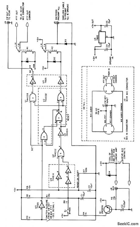
This circuit is useful in amateur radio VHF and UHF work where a mast-mounted antenna preamp is used for receiving. The kit controls T-R switching and change-over relay sequencing so that high RE levels are prevented from accidentally being applied to the preamplifier during switching intervals. (View)
View full Circuit Diagram | Comments | Reading(0)
PROGRAMMABLE_CURRENT_TO_VOLTAGE_CONVERTER
Published:2009/6/23 1:38:00 Author:May

Programmable current-to-voltage converter permits you to electrically select from 16 resistor values using bilateral switches.
IC1 741 op amp (or similar)IC2 CD4066 quad bilateral switchC1 0.1-μF capacitorR1 10-kΩ 1/4-W 5% resistorR2 4.7-kΩ, 1/4-W 5% resistorR3 2.2-kΩ, 1/4-W 5% resistorR4 1.2-kΩ, 1/4-W 5% resistorR5 100-Ω, 1/4 5% resistor (View)
View full Circuit Diagram | Comments | Reading(1045)
TEA2260 thick film switching power IC diagram
Published:2011/7/27 21:19:00 Author:Ecco | Keyword: thick film , switching power IC


TEA2260 thick film switching power integrated circuit produced by French Thomson company is widely used in large-screen color television sets and computer monitors, switching power supply circuits. 1.The internal block diagram The internal block diagram of TEA2260 integrated circuit is shown in Figure 1. 2. pin functions and data TEA2260 IC uses 16-pin double row package, and the pin functions and data are listed in Table 1.
(View)
View full Circuit Diagram | Comments | Reading(1073)
VARIABLE_FREQUENCY_ASTABLE_I
Published:2009/6/23 1:37:00 Author:May

This Circuit is a variable frequency oscillator usming a trimmer capacitor or a three-gauge AM broadcast capacitor salvaged from an old AM radio. The there sections must be paralleled. (View)
View full Circuit Diagram | Comments | Reading(829)
TWO_METER_PREAMPLIFIER_FOR_HANDITALKIES
Published:2009/6/23 1:37:00 Author:May

This simple, inexpensive, wideband rf amplifier provides 14 dB gain on two meters without the use of tuned circuits. (View)
View full Circuit Diagram | Comments | Reading(777)
Three-band graphic equalizer
Published:2011/7/28 20:34:00 Author:Ecco | Keyword: Three-band graphic equalizer

Using a single op-amp this easy to make equalizer offers three ranges, low frequency,mid frequency,and high. With component values shown there is approximately +/-20dB of boost or cut at frequencies of 50Hz, 1kHz and 10kHz. Supply voltage may be anything from 6 to 30 Volts. Maximum boost 20dB is only realized with maximum supply voltage. (View)
View full Circuit Diagram | Comments | Reading(982)
CW_SIGNAL_PROCESSOR
Published:2009/6/23 1:36:00 Author:May

This circuit provides interferenced rejection for the CW operator. The 567 phase-locked loop is configured to respond to tones from 500 to 1100 Hz. The Schmitt trigger reduces the weighting effect caused by the output of the PLL remaining low after removal o f the audio signal. Ten to 15 millivolts of audio activate the circuit. For periods of loss of signal, circuit B will automatically switch back to live receiver audio after a suitable delay. (If a relay with a 5-volt coil is not available, the circuit can also be powered from +12 volts.) When circuit B is used, the contacts on relay K1 replace S1. (View)
View full Circuit Diagram | Comments | Reading(1015)
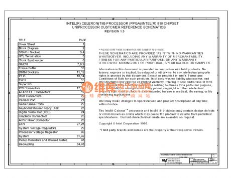
Computer motherboard circuit diagram 440LX2_27
Published:2011/7/28 22:23:00 Author:Ecco | Keyword: Computer motherboard
View full Circuit Diagram | Comments | Reading(475)
LOW_FREQUENCY_CONVERTER
Published:2009/6/23 1:35:00 Author:May

This converter circuit translates the 350-to 500-kHz range to 4.35 to 4.50 MHz,enabling thefrequency range to be received on a conventionalshortwave recelver (View)
View full Circuit Diagram | Comments | Reading(899)
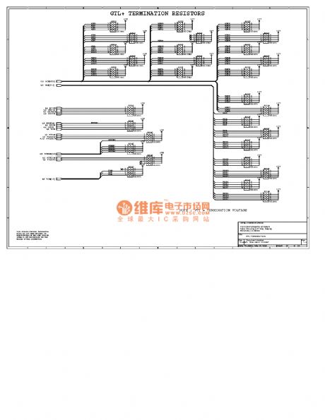
Computer motherboard circuit diagram 810 1_01
Published:2011/7/28 20:27:00 Author:Ecco | Keyword: Computer motherboard
View full Circuit Diagram | Comments | Reading(494)
Computer motherboard circuit diagram 810 1_02
Published:2011/7/28 20:28:00 Author:Ecco | Keyword: Computer motherboard
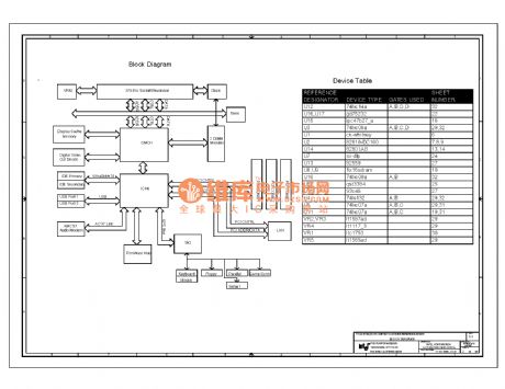
View full Circuit Diagram | Comments | Reading(599)
| Pages:1376/2234 At 2013611362136313641365136613671368136913701371137213731374137513761377137813791380Under 20 |
Circuit Categories
power supply circuit
Amplifier Circuit
Basic Circuit
LED and Light Circuit
Sensor Circuit
Signal Processing
Electrical Equipment Circuit
Control Circuit
Remote Control Circuit
A/D-D/A Converter Circuit
Audio Circuit
Measuring and Test Circuit
Communication Circuit
Computer-Related Circuit
555 Circuit
Automotive Circuit
Repairing Circuit