
Circuit Diagram
Index 1363
VCDO_II
Published:2009/6/23 4:41:00 Author:Jessie

The output frequency of this simple low-cost active voltage-controlled oscillator circuit is based upon the inherent frequency dependent characteristics of our operational amplifier.
The oscillator circuit shown uses a TL082 op amp. When power is applied, the circuit generates a sinusoidal wave. The frequency of oscillation can be changed by varying the bias supply. (View)
View full Circuit Diagram | Comments | Reading(757)
The gas overranging alarm miner lamp 4
Published:2011/7/29 2:59:00 Author:Ecco | Keyword: gas overranging, alarm , miners lamp

The working principle: The gas overranging alarm miner lamp circuit is composed of gas detection circuit, multivibrator, audio output circuit and lighting circuit. It's shown as the figure 8-32.
Gas detection circuitis composed ofthe gas sensor and resistors R2, R3.
Multivibrator is composed oftwo NAND gates Dl, D2 of internal NAND gate and resistors R4 and R5, capacitor C2.
Audio output circuit consists of resistors R6, audio amplification V and speaker BL.
Lighting circuit is composed of the battery GB, lights EL andK light switch.
When the indoor concentration of combustible gasis inthe allowable range (less than limit value), the resistance between the gas sensors A, B is high,the foot voltage of Ic is low, multivibrator does not work, the speaker BL has no sound. When the indoor concentration of combustible gasis over the limit, the resistance between the gas sensors A, B declines,the foot voltage of Ic is higher than conversion voltage of D1, multivibrator works,the output oscillation signal frompin 4of IC. The signal amplified by the V will promote the speaker BL.
(View)
View full Circuit Diagram | Comments | Reading(1223)
MULTIPLE_ON_CARD_REGULATOR_ADJUSTER
Published:2009/6/23 4:41:00 Author:Jessie

This circuit allows one pot to control several on-card regulators for adjustment within ±100 mV of each other. (View)
View full Circuit Diagram | Comments | Reading(536)
MODEL_RAILROAD_TRACK_CONTROL_SIGNAL
Published:2009/6/23 4:30:00 Author:May

When a train passesS1 (a red switch), a small magnet glued to the underside operates Sl and causes UI to generate a pulse, activating relay K1 and changing the signal from green to red. After a time determined by RI and C1 (see table), the relay de-energizes and the signal goes back to green. (View)
View full Circuit Diagram | Comments | Reading(0)
FIRE_SIREN
Published:2009/6/23 4:41:00 Author:Jessie

IC1 is an LF oscillator that is variable in attack and decay time with RI and R2. The LF output modulates HI' oscillator IC2. R5 varies the modulation depth. By proper control adjustment, sirens of various types can be simulated. (View)
View full Circuit Diagram | Comments | Reading(1)
MODEL_RAILROAD_CROSSING_FLASHER
Published:2009/6/23 4:27:00 Author:May

Gate U1-c is set up as an oscillator whose frequency is determined by C1 and R1. Gates U1-b and U1-d are set up as an RS flip-flop that is gated on by U1-a. Gate U1-a in conjunction with Q1 operates as the control gate for the flip-flop. Components D1, C2, and lR5 act as a delay circuit to compensate for anylight getting throughthe gaps between cars as theypass over the phototransistors. The light-emitting diodes are connected so that they operate alternately, depending on the outputs of U1-d and U1-b.Basically, R6 is adjusted so that ambient room-light striking Q1(and any other phototransistors connected in series)keeps the output of U1-a at pin 3 low. When a car passes over the phototransis-tor, which is installed between ties in the track, pin 3 goes high, allowing a high to be placed on pins 5 and 13. That allows the high output of UI-c at pin 10 to enable pin 12, which in turn allows pin 11 to go low. That makes a complete path for LED2 to operate. When pin 10 goes low, pin 11 goes high.That makes pin 5 high, and thus, enables pin 4 to go low and completes the circuit for LED1. That alternates the LEDs, which are installed in a railroad-crossing signal. (View)
View full Circuit Diagram | Comments | Reading(2010)
SWITCHED_POWER_CONTROL_CIRCUITS
Published:2009/6/23 4:40:00 Author:Jessie

Load currents of a few milliamperes to amperes can be turned on and off by these switched power-control circuits. The U2 CMOS inverter stage works as a simple power switch for load currents less than 5 mA (Fig. 68-27A), allowing easy reference shutdown. If appreciably higher switched output currents are called upon, an alternate CMOS inverter driving a low-threshold PMOS device can be used to switch currents of up to 1 A or more (Fig. 68-27B). (View)
View full Circuit Diagram | Comments | Reading(604)
VCO_I
Published:2009/6/23 4:39:00 Author:Jessie

This circuit gtves both triangle-and scluarewave outputs,The frequency range IS determined by C1 (View)
View full Circuit Diagram | Comments | Reading(3563)
SHORTWAVE_CONVERTERS_FOR_SCANNERS
Published:2009/6/23 4:39:00 Author:Jessie
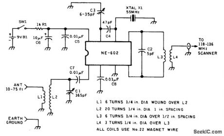
The AM aircraft band at 118 to 136 MHz is used in this converter design as an IF output The second harmonic ofthe 55 MHz crystal(110 MHz) mixes with the shortwave input of 8 to 36 MHz.AnNE602 IC IS used for the mlxer Sensitivity IS about 3μV. If desired,a crystal tuning circuit for finetuning can be obtained ustng a varactor (View)
View full Circuit Diagram | Comments | Reading(1928)
4_TO_70_V_REGULATOR
Published:2009/6/23 4:39:00 Author:Jessie

This regulator operates from a single supply.If the op amp is not able to control an overvoltage condition, the SCR will crowbar the output. (View)
View full Circuit Diagram | Comments | Reading(638)
SINE_WAVE_VCO
Published:2009/6/23 4:38:00 Author:Jessie

A dc control voltage varies the effective network C4/C3/C1 and R12/R3. Q2/Q3 are the oscillator transistors. (View)
View full Circuit Diagram | Comments | Reading(793)
33_V_SWITCHING_REGULATOR
Published:2009/6/23 3:59:00 Author:May


For the LT1129-3.3, dissipation amounts to a little under 1.5 W at full output current. The 5-lead surface-mount DD package handles this without the aid of a heatsink, provided that the device is mounted over at least 2500 mm2 of ground or power-supply plane. Efficiency is around 62%; dissi-pation in linear regulators becomes prohibitive at higher current levels, where they are supplanted by high-efficiency switching regulators. The synchronous buck converter is implemented with an LTC1148-3.3 converter. The LTC1148 uses both Burst ModeTM operation and continuous, constant off-time control to regulate the output voltage, and maintain high efficiency across a wide range of output loading conditions. (View)
View full Circuit Diagram | Comments | Reading(0)
SCANNER_SILENCER
Published:2009/6/23 4:38:00 Author:Jessie
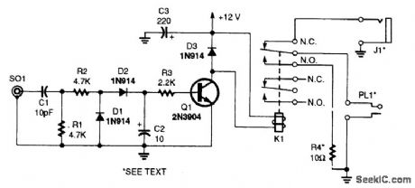
When a scanner is used at amateur radio or CB stations, the scanner sometimes picks up trans-mitted signal and howls or squeals. When RF is detected, Q1 tums on, energizing K1 and discon-necting the scanner speakers. SO1 is connected to the transmit antenna lead via a tee fitting. C1 is optimum for 5- to 10-W 30-MHz use. For higher power or higher frequencies, reduce C1 to as low as needed. If C1 is so small as to be impractical, R1 can be shunted with a 10- or 22-pF capacitor, as needed. (View)
View full Circuit Diagram | Comments | Reading(648)
VIDEO_MASTER
Published:2009/6/23 3:58:00 Author:May

The video master consists of a series of converters that place all your video sources on unused UHF channels, which then combines them with normal TV channels (terrestrial or cable into one ca-ble). That one cable can then feed several TV sets for whole-house coverage. The desired video source is selected with the TV set's tuner. All of the TV's remote-control features are retained.A complete kit of parts is available from North Country Radio, P.O. Box 53, Wykagyl Station, New Rochelle, NY 10804-0053A. (View)
View full Circuit Diagram | Comments | Reading(0)
FM_SCANNER_NOISE_SQUELCH
Published:2009/6/23 4:37:00 Author:Jessie
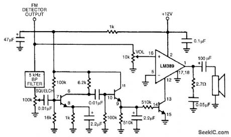
The LM389 is operated in the cut-off mode with pin 12 grounded via one of the internal transistors. A sample of detected noise is taken through a 5-kHz filter. Upon reception of signal, the detec-tor output quiets, and noise level drops. This increases impedance at pin 12 of the LM389, causing audio to be passed. The three transistors are part of the LM389. (View)
View full Circuit Diagram | Comments | Reading(1654)
1IC_REGULATOR_PROTECTION
Published:2009/6/23 3:56:00 Author:May

This circuit protects an IC regulator against various fault conditions. (View)
View full Circuit Diagram | Comments | Reading(0)
MOISTURE_DETECTOR
Published:2009/6/23 3:55:00 Author:May
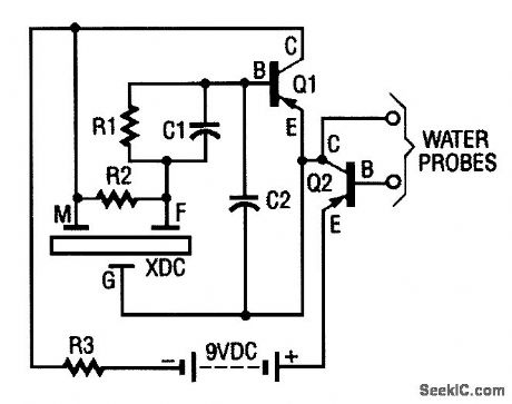

The moisture detector uses two transistors and a piezoelectric transducer to sound an alarm tone when water is present. Transistor Q1 forms a crystal-controlled oscillator, using a portion of piezoelectric transducer XDC-which contains two piezoelectric crystal regions-as the crystal. The transducer has three separate leads, One lead goes to each of the crystals, and the third lead is com-rnon to both.
The smaller internal crystal region sets the frequency of operation and the larger element is driven by Q1 (when it is biased on ) to provide the loud tone output. To turn the pnp transistor Q1 (used as an oscillator) on pnp transistor Q2 (used here as a switch) must be on. To turn it on with the biasing that is normally connected, you would only need to connect a resistor from the collector of Q2 to the base, which gives the base a negative (-) bias. The resistor used is the water that is to be detected. That turns Q2 on, which, in turn, turns on Q1. The result when water touches the probe is that the transducer emits a loud sound. (View)
View full Circuit Diagram | Comments | Reading(0)
12_V_SUPPLY
Published:2009/6/23 4:37:00 Author:Jessie

When driving a power MOSFET from a 5-V or 3.3-V system, a significant number of components usually are needed to generate an extra +12 V.It's possible, however, to apply the second channel in a typical dual MOSFET driver to derive a +12-V power supply. By using a driver with the drains brought to separated pins, you can connect an inductor between the n-channel drain and the logic supply without connecting the p-channel device.The driver operates as a standard flyback-style switched-mode circuit (see the figure). When the output n-channel device is on, current starts flowing in the inductor, which stores energy. When the n-channel device is turned off, current must continue flowing. Therefore, it flows through diode D2 to charge up C1 and C2. As the cycle repeats, the C1 and C2 voltage rises until the Zener diode prevents further voltage rise. This is needed to prevent the driver's derived supply from exceeding the part's maximum voltage rating. (View)
View full Circuit Diagram | Comments | Reading(603)
10_Hz_TO_10_kHz_3_DECADE_VCO
Published:2009/6/23 4:37:00 Author:Jessie
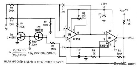
View full Circuit Diagram | Comments | Reading(1199)
IC_REGULATOR_PROTECTION
Published:2009/6/23 3:55:00 Author:May
This circuit protects an IC regulator against various fault conditions. (View)
View full Circuit Diagram | Comments | Reading(0)
| Pages:1363/2234 At 2013611362136313641365136613671368136913701371137213731374137513761377137813791380Under 20 |
Circuit Categories
power supply circuit
Amplifier Circuit
Basic Circuit
LED and Light Circuit
Sensor Circuit
Signal Processing
Electrical Equipment Circuit
Control Circuit
Remote Control Circuit
A/D-D/A Converter Circuit
Audio Circuit
Measuring and Test Circuit
Communication Circuit
Computer-Related Circuit
555 Circuit
Automotive Circuit
Repairing Circuit