Circuit Diagram
Index 1375
REINARTZ_OSCILLATOR
Published:2009/6/23 2:09:00 Author:Jessie

This oscillator uses mauctivity coupled emitter and collector windings to its main tank circuit.Take care so that L1 and L2 are not coupled to each other, otherwise this circuit is susceptible to parasitic at other frequencies.Typically ,L1 has 5 to 10 times the number of turns that L2 has.L1,L2,L3 are woundon same coil form. This oscillator is more suited to lower frequencies,≤10 MHz. (View)
View full Circuit Diagram | Comments | Reading(1705)
AUDIO_MIXER
Published:2009/6/23 1:49:00 Author:May

The 741 op amp is used as a summing amplifier to combine several audio inputs. Overall gain is set by Rf. (View)
View full Circuit Diagram | Comments | Reading(0)
PSEUDO_RANDOM_BIT_SEQUENCE_GENERATOR
Published:2009/6/23 2:09:00 Author:Jessie

In this circuit, an additional exclusive-OR gate is connected after the modulo-2 feedback, with C1 and R2 applying the supply turn-on ramp into the feedback loop. This provides sufficient transient signal so that the PRBS generator can self-start a power-up. A shift-register length n of 10 is shown with feedback at stages 3 and 10, providing true and inverted maximal length sequence outputs.
This technique applies an input directly to the feedback loop. Therefore, it's considered more reliable than applying an RC configuratior) to the shift-register reset input to create a random turnon state. (View)
View full Circuit Diagram | Comments | Reading(3645)
FET_VXO_CIRCUIT
Published:2009/6/23 1:49:00 Author:May

An MPF 102 is used in a Colpitts-type oscilla-tor in order to pull the crystal frequency slightly. (View)
View full Circuit Diagram | Comments | Reading(0)
dc_OUTPUT_CHOPPER
Published:2009/6/23 1:49:00 Author:May

Any dc voltage source in the 2- to 15-V range can be chopped into a unipolar square wave that has a peak amplitude nearly equal to the dc source voltage with circuit (lightly loaded CMOS will swing within a few millivolts of each rail at low frequencies). Depending on the actual voltage of the supply, the programmable-unij unction-transist or (PUT) relaxation oscillator produces 2000-Hz trigger pulses. These pulses operate the cascaded 74C107 flip-flop, producing a square wave. (View)
View full Circuit Diagram | Comments | Reading(0)
PROGRAMMABLE_GAIN_NONINVERTINGAMPLIFIER_WITH_SELECTABLE_INPUTS
Published:2009/6/23 2:08:00 Author:Jessie
View full Circuit Diagram | Comments | Reading(989)
ABSOLUTE_VALUE_AMPLIFIER
Published:2009/6/23 2:07:00 Author:Jessie

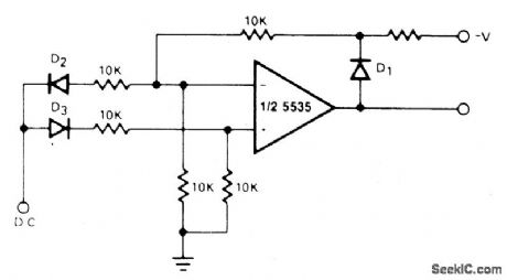
The circuit generates a positive output voltage for either polarity of input. For positive signals, it acts as a noninverting amplifier and effective. The accuracy is poor for input voltages under 1 V, but for less stringernt applications, it can ve effective. (View)
View full Circuit Diagram | Comments | Reading(1587)
AM_OSCILLATOR_FOR_WIRELESS_MICROPHONES
Published:2009/6/23 2:05:00 Author:Jessie

This circuit will generate an AM-modulated signal in the AM broadcast band that can be picked up on a receiver.About 2V of audio input will produce about 30% modulation of the oscillator signal.An old AM broadcast oscillator coil or other two-winding coil with about a 10:1 turn ratio and about 50 to 150 μH inductance can be used for T1. (View)
View full Circuit Diagram | Comments | Reading(1351)
CRYSTAL_OSCILLATOR_I
Published:2009/6/23 1:49:00 Author:May

In this circuit, series-resonant crystal XTAL1 is used as a frequency-determining element.XTAL1 is between 0.1 to 10 MHz. (View)
View full Circuit Diagram | Comments | Reading(0)
VOLTAGE_CONTROLLED_AMPLIFIER
Published:2009/6/23 2:04:00 Author:Jessie

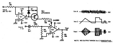
This circuit is basically an op amp with an extra input at pin 5. A current Ltac is injected into this input and this controls the gain of the device linerly. Thus by inserting an audio signal (±10 mV) between pin 2 and 3 and by controlling the current on pin 5, the level of the signal output (pin 6) is controlled. (View)
View full Circuit Diagram | Comments | Reading(2883)
PRECISION_PROCESS_CONTROL_INTERFACE
Published:2009/6/23 2:03:00 Author:Jessie
View full Circuit Diagram | Comments | Reading(863)
QUADRATURE_WAVE_OSCILLATOR
Published:2009/6/23 1:49:00 Author:May


By using a high-frequency quad current-feedback amplifier (the HA5025) as an RC oscillator, four quadrature sine waves can be generated. The HA5025's four separate amplifiers generate the sine waves, and the quad NAND gate, U2, is biased at its threshold, so it acts as a sine-wave to square-wave converter when the she waves are ac coupled into its input. (View)
View full Circuit Diagram | Comments | Reading(0)
1_dB_PAD
Published:2009/6/23 2:03:00 Author:Jessie

The 1-dB pad is useful as a termination in RF work to limit possible mismatch range between system blocks, etc. (View)
View full Circuit Diagram | Comments | Reading(1013)
SUBAUDIBLE_TONE_ENCODER
Published:2009/6/23 1:48:00 Author:May

This twin-T oscillator produces six preset subaudible tones from 93 to 170 Hz in three ranges. (View)
View full Circuit Diagram | Comments | Reading(0)
FET_QUARTZ_CRYSTAL_OSCILLATOR
Published:2009/6/23 1:48:00 Author:May

This oscillator uses an MPF102 JFET as an active element. (View)
View full Circuit Diagram | Comments | Reading(0)
SWR_WARNING_INDICATOR
Published:2009/6/23 1:47:00 Author:May

Op amp with dc input from SWR metercan be adjusted to preset the SWR reading at which the LED lights. (View)
View full Circuit Diagram | Comments | Reading(1452)
CODE_PRACTICE_OSCILLATOR_1
Published:2009/6/23 1:46:00 Author:May

Oscillator, works with 2 to 12 Vdc (but 9 to 12 volts gives best volume and clean keying). R1 can be replaced with a 500 K pot and the circuit wili sweep the entire audio frequency range. (View)
View full Circuit Diagram | Comments | Reading(0)
REMOTE_RE_CURRENT_READOUT
Published:2009/6/23 1:45:00 Author:May

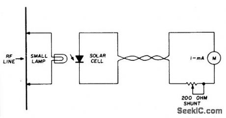
A suitable pilot lamp is illuminated by a small sample of rf and energizes an inexpensive solar cell; the dc current generated by the cell is a measure of relative rf power, and may be routed to a low-current meter located at any convenient point. A sensitive, low-current pilot lamp is desirable to cause minimum dis-turbance to normal rf circuit conditions. The number 48 or 49, 60 mA lamp is suitable for use with transmitters above 1-watt output. (View)
View full Circuit Diagram | Comments | Reading(0)
SELF_POWERED_CW_MONITOR
Published:2009/6/23 1:44:00 Author:May

Position L near the transmitter output tank to hear the key-down tone。Then tape the coil In place. C=.047μF,R=8.2 K,Q=HEP 253(or equal),T=500:500 ohm center tapped transformer. L = 2 to 6 turns on 1/2'' coil from. (View)
View full Circuit Diagram | Comments | Reading(997)
OUTPUT_TO_CURRENT_CONVERTER
Published:2009/6/23 1:44:00 Author:May

Occasionally, it is preferable to generate a cur-rent, rather than a voltage, output into the load.The availability of differential inputs aJlows this to be accomplished in any of the four basic modes.If the output is to integrated, ZL can be sim-ple high-quality capacitor, unloaded by an op amp connected as a high-impedance follower.Note that, if desired, one side of a rest switch can be grounded.The compliance constraint for this configura-tion, where VL is an arbitrary common-mode po-tential, is: |VL+IOUT(ZL+RS)|≤12V (View)
View full Circuit Diagram | Comments | Reading(0)
| Pages:1375/2234 At 2013611362136313641365136613671368136913701371137213731374137513761377137813791380Under 20 |
Circuit Categories
power supply circuit
Amplifier Circuit
Basic Circuit
LED and Light Circuit
Sensor Circuit
Signal Processing
Electrical Equipment Circuit
Control Circuit
Remote Control Circuit
A/D-D/A Converter Circuit
Audio Circuit
Measuring and Test Circuit
Communication Circuit
Computer-Related Circuit
555 Circuit
Automotive Circuit
Repairing Circuit

