
Circuit Diagram
Index 1374
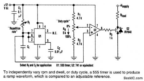
VARIED_REP_RATE_DUTY_CYCLE_WITH_555
Published:2009/6/23 1:57:00 Author:May
View full Circuit Diagram | Comments | Reading(2488)
FREQUENCY_DOUBLER_AND_CRYSTAL_OSCILLATOR
Published:2009/6/23 1:56:00 Author:May

This frequency doubler produces a sine wave at twice the frequency of XTALl. Notice that the output is taken only from OUT B (pin 5), while OUT A (pin 4) is left open. (View)
View full Circuit Diagram | Comments | Reading(1070)
50%DUTY_CYOLE_555_CIRCUIT
Published:2009/6/23 1:56:00 Author:May

Using an external charge transistor and diode enables a 50% duty cycle and easy frequency control. When the 555's discharge transistor is cut off, the 2N2222 acts as an emitter follower. When the discharge transistor turns on, the 2N2222 turns off and C1 discharges through (R1+R2) at the same rate. The IN4l48 provides temperature compensation. (View)
View full Circuit Diagram | Comments | Reading(1264)
VOLTAGE_CONTROLLED_VARIABLE_GAIN_AMPLIFIER
Published:2009/6/23 1:56:00 Author:May
The tee attenuator provides for optimum dynamic linear range attenuation up to 100 dB, even at f = 10.7 MHz with proper layout. (View)
View full Circuit Diagram | Comments | Reading(2728)
UNITY_GAIN_FOLLOWER
Published:2009/6/23 1:55:00 Author:May
View full Circuit Diagram | Comments | Reading(599)
ac_LINE_VOLTAGE_BOOSTER
Published:2009/6/23 1:54:00 Author:May

When incoming ac power drops, you can bring the voltage back up with this booster circuit. It adds the transformer's secondary voltage to the ac line voltage. (View)
View full Circuit Diagram | Comments | Reading(1253)
DIGITALLY_CONTROLLED_SQUARE_WAVE_OSCILLATOR
Published:2009/6/23 1:54:00 Author:May


IC1 LM3909 LED flasher/oscillator IC2 CD4066 quad bilateral switch C1,C2 0.1-μF capacitorC3 0.033-μF capacitorC4 0.047-μF capacitor
C5,C6 0.1-μF capacitorR1 2.2-kΩ, 1/4-W 5% resistorR2 10-kΩ potentiometerR3 2.7-kΩ, 1/4-W 5% resistorR4 470-Ω, 1/4-W 5% resistor (View)
View full Circuit Diagram | Comments | Reading(1182)
HIGH_IMPEDANCE_DIFFERENTIAL_AMPLIFIER
Published:2009/6/23 1:54:00 Author:May

View full Circuit Diagram | Comments | Reading(1471)
CRYSTAL_OSCILLATOR_WITH_ADJUSTABLE_FREQUENCY
Published:2009/6/23 1:53:00 Author:May

In this crystal oscillator circuit, C3 adjusts the frequency of the oscillator for exact netting. The crystal is a fundamental type. C1= 100 pF and C2 = 1000 pF are typicd. (View)
View full Circuit Diagram | Comments | Reading(1028)
AUTOMATIC_TTL_MORSE_CODE_KEYER
Published:2009/6/23 1:53:00 Author:May

Automatic'any generated dits and dahs are produced over a speed range of 11 to 39 wpm. The upper limit can be raised by decreasing R2. SW1 and SW2 can be a home, brew paddle operated key. (View)
View full Circuit Diagram | Comments | Reading(521)
dc_SWITCHED_CRYSTAL_OSCILLATOR
Published:2009/6/23 1:53:00 Author:May

This circuit is useful where several different crystal frequencies must be switched using a dc source. The values shown are typical for 40- to 60-MHz third-overtone crystals. Limitation on number of crystals depends on PIN diode capacitance and layout factors, but up to 5 or 10 crystals is possible. (View)
View full Circuit Diagram | Comments | Reading(655)
ac_ISOLATION_TRANSFORMERS_USE_INEXPENSIVE_12_V_TRANSFORMERS
Published:2009/6/23 1:52:00 Author:May

“Safety first”is a good motto to follow whenyou play vith electricity.You can follow thatadage more closely with this homebrew isolationtransformer (View)
View full Circuit Diagram | Comments | Reading(781)
CRYSTAL_OSCILLATOR_Ⅱ
Published:2009/6/23 1:51:00 Author:May

An NE602 can be used as a crystal oscillator. (View)
View full Circuit Diagram | Comments | Reading(1026)
HARMONIC_GENERATOR
Published:2009/6/23 1:51:00 Author:May
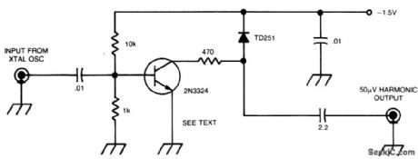
This circuit will produce 50 μV harmonics through 1296 MHz with an input of 0.15-1 V from a 100 or 1000 kHz crystal oscillator. With a germanium diode instead of a tunnel diode, harmonics can be heard up to about 147 MHz. (View)
View full Circuit Diagram | Comments | Reading(1)
Voltage-controlled duty cycle oscillator
Published:2011/7/28 2:13:00 Author:Ecco | Keyword: Voltage-controlled , duty cycle oscillator
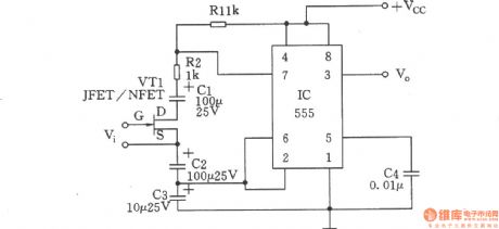
The circuit shown as the chart is a self-excited multivibrator composed of 555 timer. FET VTl is used as voltage-controlled resistor(VVR). By changing the source voltage VGS between a gate, you can change the resistance between JEFT drain (D) and source (S). Two coupling capacitors Cl and C2 can avoid the rest of the DC voltage from affecting on VTl. The value of the coupling capacitors Cl and C2should be10 times of timing capacitor, that will keep the coupling capacitor charging and discharging time from the influence of 555 timer. And at the same time, it will get a voltage variable resistor RDS between the D and S poles of VT1, and produce an empty cycle changing with VGS. RDS can reach 100kΩ. In order to obtain the maximum duty cycle variation, R2's value should take less. (View)
View full Circuit Diagram | Comments | Reading(1193)
500_ksps_8_CHANNEL_DATA_DCQUISITION_CIRCUT
Published:2009/6/23 2:10:00 Author:Jessie

The high input impedance of the LTC1278 allows multiplexing without abuffer amplifier. Both sin-gle channel and multiplexed high-speed data acquisition systems benefit from the LTC1278/LTC1279's dynamic conversion performance. The 1.6-μs and 1.4-μs conversion and 200-ns and 180-ns S/H acquisition times enable the LTC1278/LTC1279 to convert a 500 ksps and 600 ksps, respectively. The figure shows a 500-ksps 8-channel data acquisition system. The LTC1278's high input impedance eliminates the need for a buffer amplifier between the multiplexer's output and the Adc's input. (View)
View full Circuit Diagram | Comments | Reading(1105)
ORYSTAL_OSCILLATOR_WITH_FM_CAPABILITY
Published:2009/6/23 1:51:00 Author:May

This crystal oscillator produces a good FM signal that can be tripled to 146 MHz and produces a clean 5-kHz deviation signal for FM voice. The bias control is adjusted for cleanest audio while the 1-to 5-pH cqil is adjusted to set the oscillator frequency to the exact setting required. (View)
View full Circuit Diagram | Comments | Reading(733)
RE_POWERED_SIDETONE_OSCILLATOR
Published:2009/6/23 1:50:00 Author:May
A sidetone oscillator is a special audio oscillator that is turned on and off with the transmitter. The oscillator is rf-driven and bat-tery operated. It uses a 555 IC timer as an astable multivibrator. Keying is accomplished by applying a positive dc potential, developed from the rf signal, to the reset terminal of the 555. (View)
View full Circuit Diagram | Comments | Reading(794)
STABILIZED_WIEN_BRIDGE_OSCILLATOR
Published:2009/6/23 1:50:00 Author:May

In this application, the AD534 is used as a vari-able-gain amplifier for the feedback signal from the output to the Y input, via the Wien bridge. The peak-rectifter and filter combination applies sufficient voltage to the X (denominator) input to maintain a stable oscillation-amplitude (with about 0.2% ripple). At startup, because X is small (divider mode), the gain is high, and the oscillation builds up rapidly. This is but one of several possible schemes, involving no extemal active elerrtents. Its forte is simplicity, rather than high performance; nevertheless, the amplitude is not greatly affected by supply and temperature variations, about 0.003 dB per volt, and 0.005 dB per degree. (View)
View full Circuit Diagram | Comments | Reading(0)
UJT_100_kHz_CALIBRATION_OSCILLATOR
Published:2009/6/23 1:49:00 Author:May

This unusual 100-kHz oscillator (whose fre-quency is determined by XTALl) can be used as a marker generator to calibrate the analog diai of a communication receiver, or its output can be fed to a divider courtter to produce a stable lower-fre-quency output for use as a clock-signal generator. (View)
View full Circuit Diagram | Comments | Reading(0)
| Pages:1374/2234 At 2013611362136313641365136613671368136913701371137213731374137513761377137813791380Under 20 |
Circuit Categories
power supply circuit
Amplifier Circuit
Basic Circuit
LED and Light Circuit
Sensor Circuit
Signal Processing
Electrical Equipment Circuit
Control Circuit
Remote Control Circuit
A/D-D/A Converter Circuit
Audio Circuit
Measuring and Test Circuit
Communication Circuit
Computer-Related Circuit
555 Circuit
Automotive Circuit
Repairing Circuit