
Circuit Diagram
Index 1342
MANUAL_CONTROL_FOR_HEATER
Published:2009/6/24 3:53:00 Author:Jessie
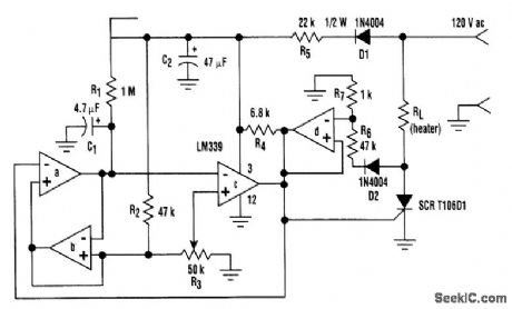
Built around an LM339 quad comparator, this circuit provides manual control of the output of a resistive heater or other load with a long time constant. The circuit's design uses minimal parts, thus it's inexpensive, and generates very low RFI.Comparators a,b, and c form a low-frequency pulse-width modulator. Sections a and b form a sawtooth oscillator (of approximately 0.25 Hz), with capacitor C1 being charged through RI and dis-charged through section a's open collector output. R2 and R3 set the upper voltage limit for the saw-tooth wave. The hysteresis means that C1 is discharged to nearly 0V, creating a voltage swing that is identical to the adjustment range of R3.Comparator c, in conjunction with potentiometer R3, converts the sawtooth wave form to a vari-able duty-cycle drive for the silicon-controlled rectifier.Increasing voltage at R3's wiper means increasing the on time. Section d holds the SCR gate low if the line voltage is above approximately 3.5 V, preventing turn on at mid-cycle and ensuring low RFI.The oscillator frequency is roughly determined by 1/0.7R1C1 Resistance R1 must be greater than 4R2 or the oscillator will lock up. ReducingR1 will increase the lower voltage limit of the sawtooth; in-creasing it might cause lock-up. (View)
View full Circuit Diagram | Comments | Reading(1705)
OPTICAL_DIRECTION_DISCRIMINATOR
Published:2009/6/24 3:53:00 Author:Jessie
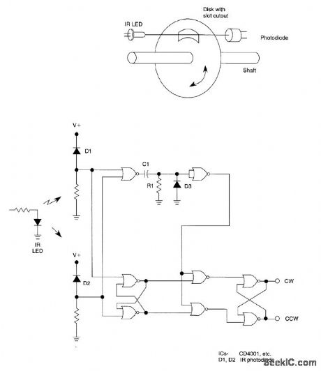
The very simple circuit uses only two CD4001 packages, i.e., eight NOR gates and operates in the following way: Pulse streams are fed to an RS flip flop generating an output waveform which has a small or large duty cycle depending on the direction of rotation. The same input pulses are also fed to a NOR gate, which adds the two pulse trains.
The rising edges of this waveform are used to produce short positive pulses from the circuit con-sisting of R1, C1, D3, and a NOR gate used as an inverter. This is used to sample the outputs of the flip flop to detect the direction of rotation. The output, whose duty cycle is large, forces the sampling NOR gate to generate a pulse train which sets (or resets) the second RS flip-flop continuously giv-ing a permanent indication of the direction of rotation. (View)
View full Circuit Diagram | Comments | Reading(487)
SHORTWAVE_RECEIVER
Published:2009/6/24 3:45:00 Author:May
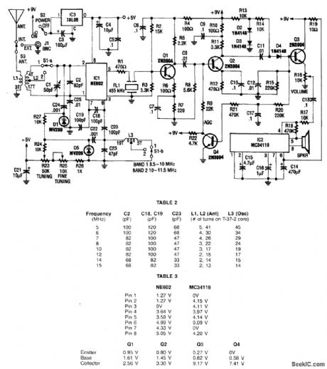
This receiver covers 8.5 to 11.5 MHz in two bands and has a sensitivity of under 1 μV. Nn NE602 mixer feeds a 455-kHz IF amplifier (Q1 and Q2), detector D4, and audio amplifier IC2. Q4 serves as an AGC amplifier coil data is given in the table. The LO is varactor tuned. (View)
View full Circuit Diagram | Comments | Reading(0)
ASTABLE_WITH_VARIABLE_PULSE_WIDTH
Published:2009/6/24 3:44:00 Author:May
This produces a positive variable width pulse and has a symmetry control. R1 and R2 control the pulse width and symmetry. (View)
View full Circuit Diagram | Comments | Reading(0)
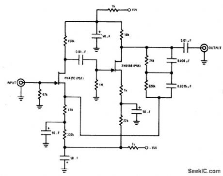
HIGH_GAIN_INVERTING_AC_AMPLIFIER
Published:2009/6/24 3:53:00 Author:Jessie
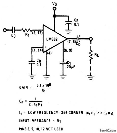
View full Circuit Diagram | Comments | Reading(512)
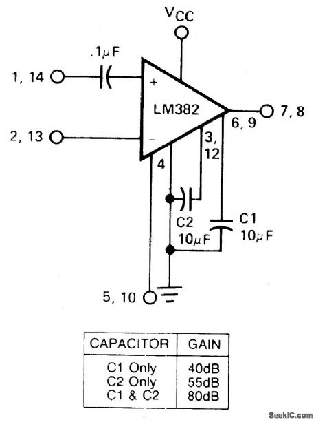
ADJUSTABLE_GAIN_NONINVERTING_AMPLIFIER
Published:2009/6/24 3:53:00 Author:Jessie
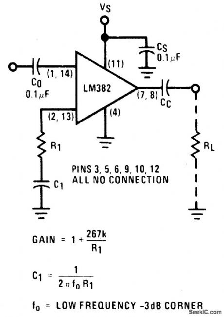
View full Circuit Diagram | Comments | Reading(564)
DISC_TAPE_PHASE_MODULATED_READBACK_SYSTEMS
Published:2009/6/24 3:44:00 Author:May
View full Circuit Diagram | Comments | Reading(0)
DUAL_INVERTER_LINE_RECEIVER
Published:2009/6/24 3:52:00 Author:Jessie
This circuit is for audio applications. (View)
View full Circuit Diagram | Comments | Reading(860)
PHONE_HELPER
Published:2009/6/24 3:44:00 Author:May

This phone-line simulator uses a 60-Hz transformer instead of a ring generator. The dial tone is provided by an NE555 astable oscillator. (View)
View full Circuit Diagram | Comments | Reading(0)
PHONE_LINE_SIMULATOR
Published:2009/6/24 3:44:00 Author:May

This device contains a ringing generator and a tone oscillator. The tone oscillator is set to either 350 or 440 Hz. The ringing generator is a potted module delivering 86 Vac at 20 Hz. It is available from a source listed in the reference. (View)
View full Circuit Diagram | Comments | Reading(1356)
MAGNETIC_PICKUP_PHON0_PREAMPLIFIER
Published:2009/6/24 3:44:00 Author:May
This preamplifier provides proper loading to a reluctance phono cartridge. It provides approximately 35 dB of galn at 1 kHz (2.2 mV input for 100 mV output).It features (S+N)/N ratio of better than -70 dB (referenced to 10 mV input at 1 kHz) and has a dynamic range of 84 dB (referenced to 1 kHz). The feedback provides for RIAA equalization. (View)
View full Circuit Diagram | Comments | Reading(806)
PHONO_[REAM_RIAA_EQUALIZATION
Published:2009/6/24 3:52:00 Author:Jessie
View full Circuit Diagram | Comments | Reading(743)
TELEPHONE_BELL_AMPLIFIER
Published:2009/6/24 3:43:00 Author:May
Telephone bell amplifier circuit will let you hear (or see) an enhanced alarm if you are away from your telephone. (View)
View full Circuit Diagram | Comments | Reading(674)
WWV_RECEIVER
Published:2009/6/24 3:43:00 Author:May
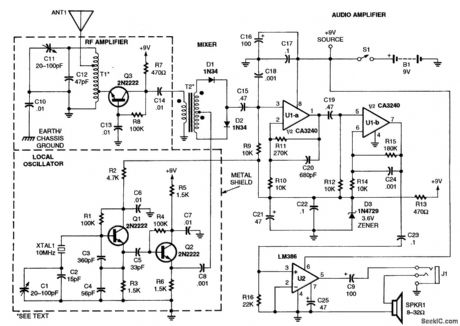
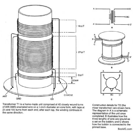
RF amplifier Q3 feeds diode mixer D1-D2 and Q1-Q2 provide 10-MHz L.O. injection to D1 through T1 and T2,U1A,U1B and U2 are audio amplifiers.Details of T1 and T2 are shown. (View)
View full Circuit Diagram | Comments | Reading(0)
REMOTE_AMPLIFIER
Published:2009/6/24 3:51:00 Author:Jessie
View full Circuit Diagram | Comments | Reading(530)
TELEPHONE_RECORDING_CIRCUIT
Published:2009/6/24 3:42:00 Author:May

This device will automatically record telephone calls. An ordinary cassette recorder can be hooked to it. (View)
View full Circuit Diagram | Comments | Reading(1016)
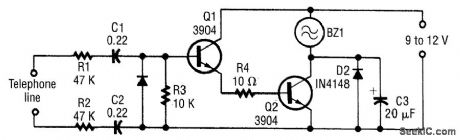
TELEPHONE_RING_AMPLIFIER
Published:2009/6/24 3:41:00 Author:May
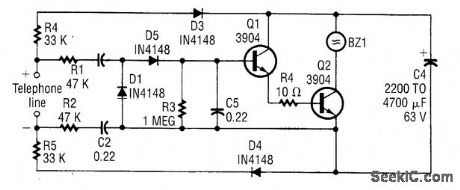
This circuit takes its operating power from the telephone line BZ1 is a piezoelectric transducer. (View)
View full Circuit Diagram | Comments | Reading(466)
ASTABLE
Published:2009/6/24 3:41:00 Author:May

At the instant that power is applied to the 555 astable, timing capacitor C1 is initially discharged, causing the output of the chip output at pin 3 to be high. Once C1 has charged to about 2/3 of the supply voltage, its output goes low, and the discharge transistor turns on, draining the charge on C1. (View)
View full Circuit Diagram | Comments | Reading(0)
UNIVERSAL_TELEPHONE_HOLD_CIRCUIT
Published:2009/6/24 3:41:00 Author:May

The telephone line is connected to the hold components through bridge rectifier BR1 so that the input is not polarity sensitive. If you have touch-tone telephone service, you can now put a call on hold from any phone in your house by plugging this simple device into any telephone jack. The uni-versal hold circuit works with any phone that has a key pad with a # key. To put a call on hold, press the # key and hang the phone up. A timer extends the #-key function while you hang up phones that have a keypad built into the handset. (View)
View full Circuit Diagram | Comments | Reading(1052)
TRANSFORME_RLESS_BALANCE_INPUTS_MICROPHONE_PREAMP
Published:2009/6/24 3:39:00 Author:May
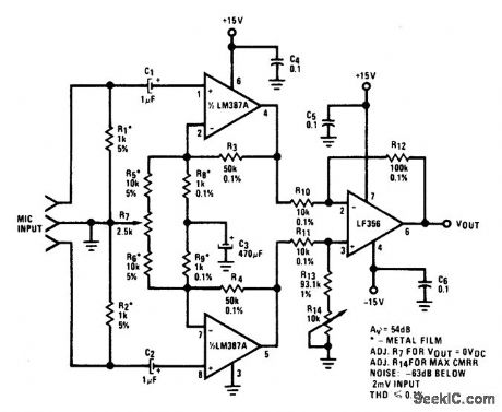
View full Circuit Diagram | Comments | Reading(1210)
| Pages:1342/2234 At 2013411342134313441345134613471348134913501351135213531354135513561357135813591360Under 20 |
Circuit Categories
power supply circuit
Amplifier Circuit
Basic Circuit
LED and Light Circuit
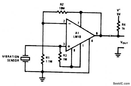
Sensor Circuit
Signal Processing
Electrical Equipment Circuit
Control Circuit
Remote Control Circuit
A/D-D/A Converter Circuit
Audio Circuit
Measuring and Test Circuit
Communication Circuit
Computer-Related Circuit
555 Circuit
Automotive Circuit
Repairing Circuit