
Circuit Diagram
Index 1347
DIGITALLY_CONTROLLED_ONE_OF_FOUR_ANALOG_SWITCH
Published:2009/6/24 3:15:00 Author:May

View full Circuit Diagram | Comments | Reading(0)
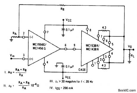
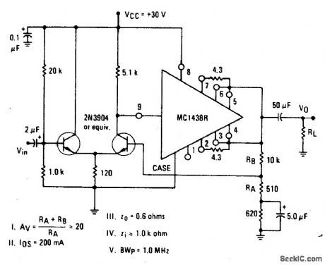
INVERTING_POWER_AMPLIFIER
Published:2009/6/24 3:14:00 Author:May

View full Circuit Diagram | Comments | Reading(1227)
RESISTOR_PIN_DIODE_SWITCH
Published:2009/6/24 3:13:00 Author:May

This circuit uses resistors instead of RE chokes to keep costs low. The values of R1 and R2 should be no lower than about 1 kΩ to minimize loss. (View)
View full Circuit Diagram | Comments | Reading(0)
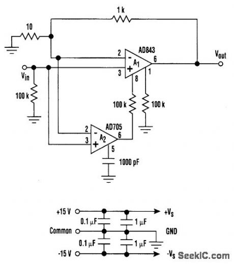
NONINVERTING_POWER_AMPLIFIER
Published:2009/6/24 3:13:00 Author:May
View full Circuit Diagram | Comments | Reading(827)
FULL_WAVE_SPEED_CONTROL_FOR_MOTORS
Published:2009/6/24 3:13:00 Author:May

A bridge rectifier provides pulsating dc to a universal motor, and the SCR is used as a phase-con-trolled switch. This circuit allows smoother operation of the motor at low speeds. (View)
View full Circuit Diagram | Comments | Reading(1566)
RECEIVER_BANDSWITCHING
Published:2009/6/24 3:13:00 Author:May

Eight-band receiver front-end selection can be accomplished by using PIN diode switches (View)
View full Circuit Diagram | Comments | Reading(595)
LOW_NOISE_AND_DRIFT_COMPOSITE_AMP
Published:2009/6/24 3:13:00 Author:May
This circuit offers the best of both worlds, It can be combined with a low input offset voltage and drift without degrading the overall system's dynamic performance. Compared to a standalone FETinput operational amplifier, the composite amplifier circuit exhibits a 20-fold improvement in voltage offset and drift.
In this circuit arrangement, A1 is a highspeed FET input op amp with a closed-loop gain of 100 (the source impedance was arbitrarily chosen to be 100 kΩ). A2 is a SuperBeta bipolar input op amp. It has good dc characteristics, biFET-level input bias current, and low noise. A2 monitdrs the voltage at the input of Al and injects current to Al's null pins. This forces A1 to have the input properties of a bipolar amplifier while maintaining its bandwidth and low-inputbias-current noise. (View)
View full Circuit Diagram | Comments | Reading(718)
POLARITY_PROTECTOR
Published:2009/6/24 3:13:00 Author:May

The use of a four-diode bridge guarantees correct polarity irrespective of input dc polarity. Remember that two diode drops (about 1.2 to 1.5 V) are lost from the input voltage using this circuit (View)
View full Circuit Diagram | Comments | Reading(768)
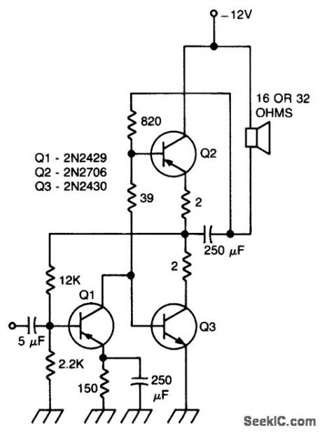
NONINVERTING_AC_POWER_AMPLIFIER
Published:2009/6/24 3:12:00 Author:May
View full Circuit Diagram | Comments | Reading(552)
SHUNT_PIN_DIODE_SWITCH
Published:2009/6/24 3:12:00 Author:May

This PlN-diode switching circuit directs sig-nals to ground when D1 is forward-biased. R1 is Lypically 470Ω to 2.2kΩ. C1 = C2 =0.1μF. (View)
View full Circuit Diagram | Comments | Reading(744)
SHORT_CIRCUIT_PROTECTION_CIRCUIT
Published:2009/6/24 3:11:00 Author:May

When S1 is pressed, the coil of K1 is energized, closing its norrrtally open contacts. If the regulated dc input is between 1 and 24 V, that voltage feeds the base of Q1 through R1, turning on the transistor, and latching the relay. When that occurs, LED2 glows indicating that all is okay.If there is a short to ground at the circuit's output (i.e., in the device being powered), the voltage that feeds the base of Q1 goes to zero, turning off the transistor. Then, LED1 glows because K1 is de-energized to indicate the short circuit. (View)
View full Circuit Diagram | Comments | Reading(914)
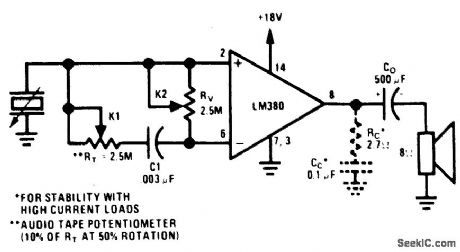
NOVEL_LOUDSPEAKER_COUPLING_CIRCUIT
Published:2009/6/24 3:11:00 Author:May

The ground side of the speaker is con-nected to the junction of two equal high value capacitors (1000 μF is typical) across the sup-ply. The amplifier output voltage will be VS/2, and so will the voltage across C1 (if C1 and C2 are equal); so as the supply voltage builds up, the dc voltage across the speaker will remain zero, eliminating the switch-on surge. C1 and C2 will also provide supply smoothing. The circuit is shown with the LM380, but could be applied to any amplifier circuit, providing that the dc voltage at the output is half the supply voltage. (View)
View full Circuit Diagram | Comments | Reading(746)
ANALOG_SWITCH
Published:2009/6/24 3:11:00 Author:May

This design takes advantage of the strobed output stage of a CA3140 amplifier. With the strobing capability, the circuit's output voltage can be set to either of the input voltages by grounding one of the control inputs, either A or B.When the strobe input at pin 8 is taken below 1V, that amplifier is disabled. The remaining am-plifier then acts as a unity-gain high-impedance buffer.The 10-kΩ output resistor enables the output voltage to swing down to 20 mV from ground. The Zener-diode clamps and associated resistors connected at the strobe inputs can be omitted for the lowest-cost applications. However, experience has shown that they allow the amplifiers to shrug off the effect of high transient voltages.The circuit is particularly suited to 8-bit microcontroller applications, where the strobe inputs can be driven directly from two open-collector output ports under software control.The use of Schottky diodes for Dl and D2 makes possible an output swing of 2.5 V when the circuit is powered from a 5-V supply. (View)
View full Circuit Diagram | Comments | Reading(1776)
470_mW_COMPLEMENTARY_SYMMETRY_AUDIO_AMPLIFIER
Published:2009/6/24 3:10:00 Author:May
This circuit has less than 2% distortion and is flat within 3 dB from 15 Hz to 130 kHz. (View)
View full Circuit Diagram | Comments | Reading(675)
8_DIGIT_100_MHz_FREQUENCY_PROBE
Published:2009/6/24 3:10:00 Author:May

Small enough to mount in a probe, this frequency counter circuit is good to 100 MHz. It operates from +5 to +15 Vdc. An 11C90 prescaler drives a 10-MHz counter chip (ICM7216B). Note the dotted line connecting R10 with pins 5 and 6 of IC2; that variable connection controls the decimal point and total count appearing on DSP1 and DSP2. The relative intensities and dura-tions of ON/OFF time for LED1 (green) and LED2 (red) give a rough indication of logic level and duty cycle. (View)
View full Circuit Diagram | Comments | Reading(7672)
PHONOGRAPH_AMPLIFIERCERAMIC_CARTRIDGE
Published:2009/6/24 3:18:00 Author:Jessie
View full Circuit Diagram | Comments | Reading(613)
SERIES_SHUNT_PIN_DIODE_RF_SWITCH
Published:2009/6/24 3:17:00 Author:Jessie

A combination of series and shunt switching, like that shown between the input and output when in the off condition. (View)
View full Circuit Diagram | Comments | Reading(1896)
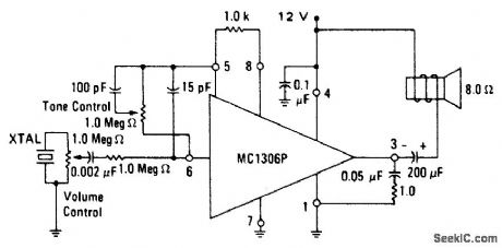
PHONO_AMPLIFIER_WITH_“COMMON_MODE”VOLUME_AND_TONE_CONTROL
Published:2009/6/24 3:17:00 Author:Jessie
View full Circuit Diagram | Comments | Reading(417)
TRANSCEIVER_T_R_SWITCH
Published:2009/6/24 3:17:00 Author:Jessie

This transceiver's transmit/receive switch uses PIN-diode instead of a relay. On receive, D1 is cut off, D2 is cut off and the antenna connects to the receiver. During transmit, D1 is forward-biased, as is D2. This connects the receiver input. This causes the input impedance of the transmission line to be high, so little transmitter power reaches the receiver. Although not shown in the schematic, the 12-V supply should have a series resistor of 100Ω to 2.2kΩ, depending on diode current, to limit diode current to a safe value. (View)
View full Circuit Diagram | Comments | Reading(1580)
DISPLAY_BOARD_FOR_RADAR_GUN
Published:2009/6/24 3:17:00 Author:Jessie

This circuit takes signal (doppler) from a radar,un, amplifies and limits it, and feeds the frequency into a counter (U4) and display circuit (DISP1, DISP2,U5,U6). Counter calibration is set by clock circuit U2B. Calibration is obtained via R21 and R22. R21 can be changed if kilometers/hour readout is desired. (View)
View full Circuit Diagram | Comments | Reading(0)
| Pages:1347/2234 At 2013411342134313441345134613471348134913501351135213531354135513561357135813591360Under 20 |
Circuit Categories
power supply circuit
Amplifier Circuit
Basic Circuit
LED and Light Circuit
Sensor Circuit
Signal Processing
Electrical Equipment Circuit
Control Circuit
Remote Control Circuit
A/D-D/A Converter Circuit
Audio Circuit
Measuring and Test Circuit
Communication Circuit
Computer-Related Circuit
555 Circuit
Automotive Circuit
Repairing Circuit