Circuit Diagram
Index 1346
ALTERNATING_ON_OFF_CONTROL
Published:2009/6/24 3:21:00 Author:May
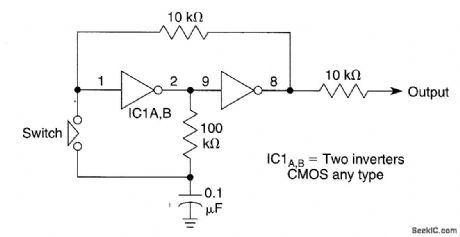
When the switch is closed, it causes a change in the state of pins 1 through 8. This will provide a toggle flip-flop action. (View)
View full Circuit Diagram | Comments | Reading(709)
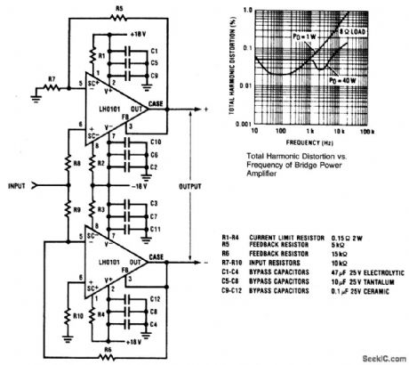
BRIDGE_AUDIO_POWER_AMPLIFIER
Published:2009/6/24 3:21:00 Author:May
View full Circuit Diagram | Comments | Reading(507)
ANALOG_SWITCH_CIRCUIT_1
Published:2009/6/24 3:24:00 Author:Jessie
View full Circuit Diagram | Comments | Reading(934)
GEIGER_COUNTER
Published:2009/6/24 3:21:00 Author:May
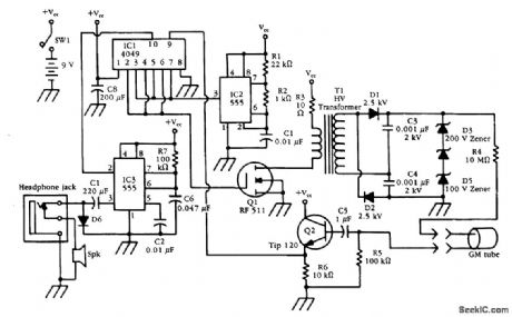
An HV generator (IC1, IC2, Q1, T1, and associated components) power a G-M tube. A pulse from the GM tube is interfaced through Q2 and IC1 to pulse generator IC3, which drives a speaker. (View)
View full Circuit Diagram | Comments | Reading(745)
TRIAC_MOTOR_CONTROL_CIRCUIT
Published:2009/6/24 3:23:00 Author:Jessie

An SCR-controlled ac motor control circuit. This is a full-wave circuit and is best used when the load remains constant. (View)
View full Circuit Diagram | Comments | Reading(4933)
SIMPLE_SWITCH_DEBOUNCER
Published:2009/6/24 3:23:00 Author:Jessie

Pressing S1 discharges C1 through R1, causing Q1 to cut off, forcing the output high. Once C1 is discharged below the VBE (ON) of Q1, switch bounce will have no effect on the output. (View)
View full Circuit Diagram | Comments | Reading(1156)
HEXFET_SWITCH_CIRCUITS
Published:2009/6/24 3:21:00 Author:May

The HEXFET can switch dc power to relays (as shown in A),motors,lamps,and numerous otherdevices That arrangement can even be used to switch resistors in and out ofa circuit,as shown in Fig.88-18B R1,R2,and R3 are possible load resistors and representload configurations that can be used (View)
View full Circuit Diagram | Comments | Reading(749)
FLYBACK_POWER_SUPPLY_FOR_RADON_MONITOR
Published:2009/6/24 3:23:00 Author:Jessie

This blocking-oscillator flyback circuit is an alternative for charging the ionization chamber capacitor. (View)
View full Circuit Diagram | Comments | Reading(2338)
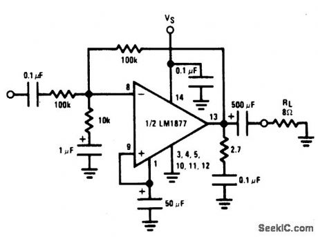
INVERTING_UNITY_GAIN_AMPLIFIER
Published:2009/6/24 3:19:00 Author:May
View full Circuit Diagram | Comments | Reading(485)
26_GHz_OSCILLATOR_FOR_RADAR_SPEED_GUN
Published:2009/6/24 3:19:00 Author:May
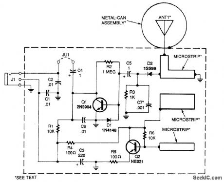
This circuit consists of 2.6-GHz oscillator Q2, a coupling rrticrostripline to ANT1, a 1.1 1/4 wave probe, detector D2, and audio amp Q1. The oscillator feeds power to the antenna, which radiates the signal. The reflected signal from a moving target mixes with the oscillator signal in D2. The resultant beat note (doppler shift) is amplified by Q1 and fed to jack J1, which is used to feed the circuit 12 Vdc. (View)
View full Circuit Diagram | Comments | Reading(2167)
SWITCH_DEBOUNCERS
Published:2009/6/24 3:22:00 Author:Jessie

These circuits will cure problems caused by switch-contact bounce. The one shown in Fig.88-21A provides you a positive output pulse, and the one shown in Fig. 88-21B provides you a neg-ative output pulse. (View)
View full Circuit Diagram | Comments | Reading(1118)
SWITCH_ON_DELAY_CIRCUIT
Published:2009/6/24 3:19:00 Author:May

When S1 is tumed on, a very small current flows through the load. Almost the entire supply volt-age appears across the SCR. When C1 changes up to the firing voltage of Q1 (approximately the standoff ratio of Q1 times VS, usually 0.4 to 0.6 VS) through R1, Q1 fires, tuming on SCR1. This deliv-ers full voltage to load, minus SCR drop (about 1.2 V). Notice that load current must exceed SCR holding current. (View)
View full Circuit Diagram | Comments | Reading(723)
AUDIO_CONTROLLED_SWITCH
Published:2009/6/24 3:22:00 Author:Jessie

The audio-controlled switch combines a pair of 741 op amps, two 2N222 general-purpose tran-sistors, a HEXFET, and a few support components to produce a circuit that can be used to turn on a tape recorder, a transmitter, or just about anything using sound. (View)
View full Circuit Diagram | Comments | Reading(2288)
SINGLE_OP_AMP_FULL_WAVE_RECTIFIER
Published:2009/6/24 3:19:00 Author:May
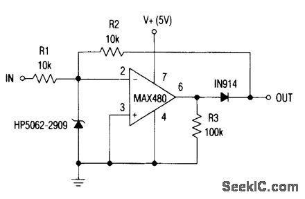
This circuit operates from +5 V and uses a single op amp to deliver a full-wave rectified output of the input signal. (View)
View full Circuit Diagram | Comments | Reading(1075)
PHONNO_AMPLIFIER
Published:2009/6/24 3:18:00 Author:May
View full Circuit Diagram | Comments | Reading(491)
AUTO_OFF_POWER_SWITCH
Published:2009/6/24 3:18:00 Author:May

This timed switch circuit can be usedwhere a timed power Source IS needed,The on-time is approximately 4.6RC (View)
View full Circuit Diagram | Comments | Reading(749)
SERIES_SHUNT_PIN_DIODE_RF_SWITCH
Published:2009/6/24 3:17:00 Author:May

A combination of series and shunt switching, like that shown between the input and output when in the off condition. (View)
View full Circuit Diagram | Comments | Reading(0)
TRANSCEIVER_T_R_SWITCH
Published:2009/6/24 3:17:00 Author:May

This transceiver's transmit/receive switch uses PIN-diode instead of a relay. On receive, D1 is cut off, D2 is cut off and the antenna connects to the receiver. During transmit, D1 is forward-biased, as is D2. This connects the receiver input. This causes the input impedance of the transmission line to be high, so little transmitter power reaches the receiver. Although not shown in the schematic, the 12-V supply should have a series resistor of 100Ω to 2.2kΩ, depending on diode current, to limit diode current to a safe value. (View)
View full Circuit Diagram | Comments | Reading(0)
DISPLAY_BOARD_FOR_RADAR_GUN
Published:2009/6/24 3:17:00 Author:May

This circuit takes signal (doppler) from a radar,un, amplifies and limits it, and feeds the frequency into a counter (U4) and display circuit (DISP1, DISP2,U5,U6). Counter calibration is set by clock circuit U2B. Calibration is obtained via R21 and R22. R21 can be changed if kilometers/hour readout is desired. (View)
View full Circuit Diagram | Comments | Reading(3493)
PIN_DIODE_SWITCH
Published:2009/6/24 3:16:00 Author:May

This PIN diode switch uses RF chokes and a single diode。R1 is typically 470Ω to 2.2kΩ (View)
View full Circuit Diagram | Comments | Reading(0)
| Pages:1346/2234 At 2013411342134313441345134613471348134913501351135213531354135513561357135813591360Under 20 |
Circuit Categories
power supply circuit
Amplifier Circuit
Basic Circuit
LED and Light Circuit
Sensor Circuit
Signal Processing
Electrical Equipment Circuit
Control Circuit
Remote Control Circuit
A/D-D/A Converter Circuit
Audio Circuit
Measuring and Test Circuit
Communication Circuit
Computer-Related Circuit
555 Circuit
Automotive Circuit
Repairing Circuit
