
Circuit Diagram
Index 1349
BASIC_ZERO_CROSSING_SWITCH_CIRCUIT
Published:2009/6/24 3:10:00 Author:Jessie

Here is the schematic of a solid-state ac relay with zero-crossing. The triac permits the relay to switch to ac directly. (View)
View full Circuit Diagram | Comments | Reading(2686)
SIMPLE_LOGIC_PROBE_WITH_ALPHANUMERIC_DISPLAY
Published:2009/6/24 3:03:00 Author:May

A logic probe also includes BCD decoder module. The red LED lights to indicate a logic high, and the green LED lights to indicate a logic low. This probe circuit will light a green (low) or red (high), and if desired, an alphanumeric display can be obtained with two 7-segment LED displays. (View)
View full Circuit Diagram | Comments | Reading(2043)
OSCILLATOR_TRIGGERED_SWITCH
Published:2009/6/24 3:09:00 Author:Jessie

In this circuit (the oscillator-triggered switch), the generated by an astable oscillator. (View)
View full Circuit Diagram | Comments | Reading(2127)
NONINVERTING_AMPLIFIER_USING_SPLIT_SUPPLY
Published:2009/6/24 3:03:00 Author:May
View full Circuit Diagram | Comments | Reading(547)
CURRENT_PROBE_AMPLIFIER
Published:2009/6/24 3:02:00 Author:May
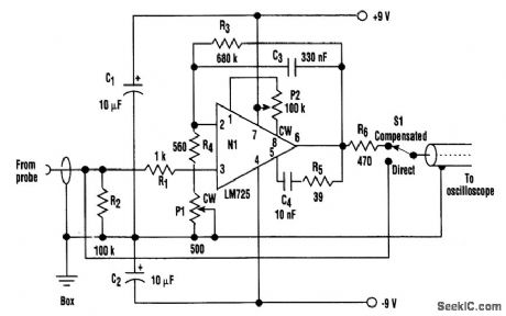
A clamp-on current probe, such as the Tektronix P6021, is a useful means of displaying current waveforms on an oscilloscope. A less-expensive and simple alternative is shown in the figure.The more sensitive range on the P6021 is 2 mA/mV, but it has a roll-off of 6-dB per octave below 450 Hz. The purpose of the compensator is to counteract the low-frequency attenuation, which is achieved by means of C3 and R4 + P1 in the feedback around op amp N1. It's important that the latter is a low-noise type, such as the LM725 shown in the figure. On top of that, it's necessary at some point to limit the increasing gain with decreasing frequency; otherwise, amplifier noise and drive will overcome the signal. The values shown for C3 and R3 give a lower limit of less than 1 Hz.A test square wave of ±1 mA is fed to the current probe so that P1 can be adjusted for minimum droop or overshoot in the output waveform. It's vital that the sliding core on the probe is fully closed. At high frequencies, the response begins to fall off at 100 kHz. Therefore, for most waveforms, switch S1 is moved to direct, above a fundamental frequency of, for example, 10 kHz.This circuit's current consumption is quite low, and it can be battery powered. If a mains power supply is built-in, it must be well screened to prevent hum problems. (View)
View full Circuit Diagram | Comments | Reading(1612)
OP_AMP_AND_ANALOG_SWITCH_RON_COMPENSATOR
Published:2009/6/24 3:08:00 Author:Jessie
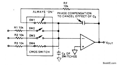
This switch is in series with feedback resistor to compensate gain. (View)
View full Circuit Diagram | Comments | Reading(0)
VARIABLE_VOLTAGE_REGULATOR_WITH_WIDE_RANGE_CURRENT_LIMITING
Published:2009/6/24 2:56:00 Author:May


In this circuit,R9 acts as a control to set current limiting。If R9=0,limiting occurs at 47 mA.Input is 24 V, output isdepending on the setting of R6. (View)
View full Circuit Diagram | Comments | Reading(827)
POWER_OP_AMP
Published:2009/6/24 3:08:00 Author:Jessie
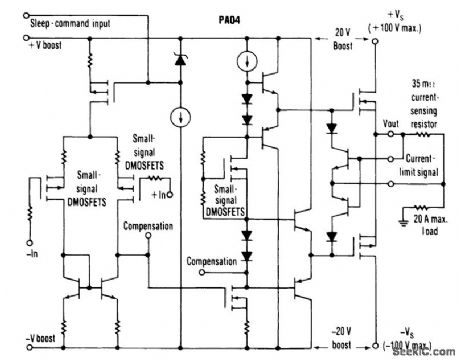
This circuit from Apex Microtechnology can deliver 180 V p-p@90 kHz into a 4-Ωload.The PA04 can deliver 400-W RMS into an 8-Ω load with low THD at frequencies beyond 20 kHz. (View)
View full Circuit Diagram | Comments | Reading(718)
-100_Vdc_SUPPLY
Published:2009/6/24 1:42:00 Author:May

The combination Hartley oscillator/step-up transformer shown in A can generate significant negative high-voltage-especially if the voltage output of the transformer is multiplied by the circuit in Fig.69-5B. T1 is a small low-voltage filament transformer of around 4- to 10-Vac output, 120-V primary. (View)
View full Circuit Diagram | Comments | Reading(903)
AM_RADIO_POWER_AMPLIFIER
Published:2009/6/24 3:08:00 Author:Jessie

View full Circuit Diagram | Comments | Reading(510)
LOW_OUTPUT_IMPEDANCE_MULTIPLEXER
Published:2009/6/24 3:08:00 Author:Jessie

Both inputs are terminated in their characteristic impedance; 75Ω is typical for video applications. Because the output cables usually are terminated in their characteristic impedance, the gain is 0.5. Consequently, amplifiers U2A and U2B are configured in a gain of +2 to set the circuit gain at 1.R2 and R3 determine the amplifier gain; if a different gain is desired, R2 should be changed according to the equation G = (1 + R3/R2) R5, LCL1, and D1 make up an asymmetrical charge/discharge time circuit that configures U1 as a break-before-make switch to prevent both amplifiers from being ac-tive simultaneously. The multiplexer transition time is approximately 15μs with the component values shown. (View)
View full Circuit Diagram | Comments | Reading(1300)
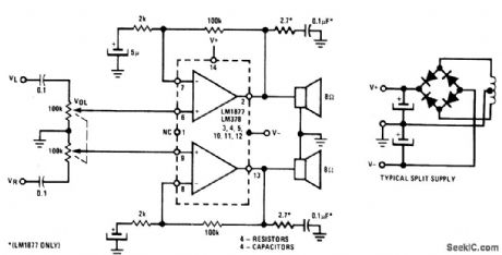
STEREO_AMPLIFIER_WITH_Av=200
Published:2009/6/24 3:08:00 Author:Jessie
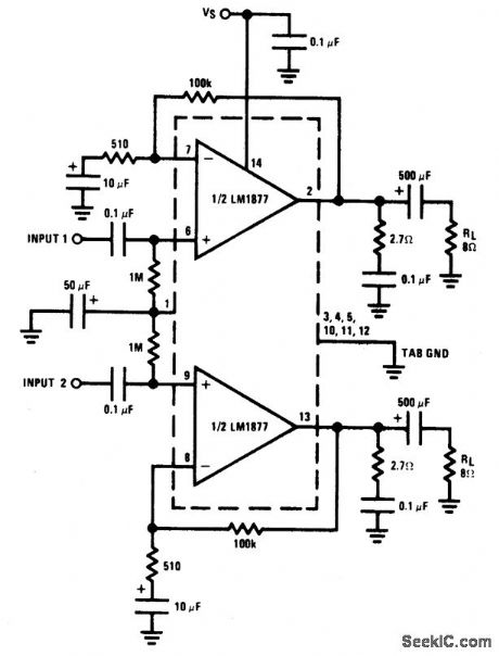
View full Circuit Diagram | Comments | Reading(600)
pH_PROBE_AMPLIFIER
Published:2009/6/24 3:07:00 Author:Jessie

The low-noise precision FET op-amp AD795 has around 1014-Ω common-mode impedance, lowoffset voltage (250 μVmax) and L13 μVC drift make this device ideal for low-voltage measurements from high-impedance sources. (View)
View full Circuit Diagram | Comments | Reading(696)
10_W_POWER_AMPLIFIER
Published:2009/6/24 3:07:00 Author:Jessie
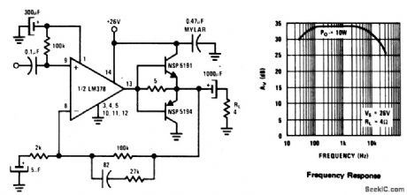
View full Circuit Diagram | Comments | Reading(1060)
125_MHz_LOGIC_PROBE
Published:2009/6/24 3:06:00 Author:Jessie

This logic probe features either high-low (LED) indication or latching operation. When S1 closed, the indication of a pulse is latched and the red LED1 stays on. Piezoelectric buzzer BZ1 used as a beeper to sound that a logic high is preset. (View)
View full Circuit Diagram | Comments | Reading(2003)
12_W_LOW-DISTORTION_POWER_AMPLIFIER
Published:2009/6/24 3:06:00 Author:Jessie
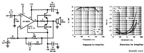
View full Circuit Diagram | Comments | Reading(532)
STEPPER_MOTOR_ENCODER_CIRCUIT
Published:2009/6/24 3:00:00 Author:May

This circuit translates shaft rotation and direction to a readout on an LED display. A stepper motor is used as an encoder. (View)
View full Circuit Diagram | Comments | Reading(0)
ADJUSTABLE_BIAS_REGULATOR
Published:2009/6/24 2:59:00 Author:May


If the wiper of R2 is set at N% rotation,the bias voltage Will be∶This method derives a bias voltage that tracks VBE of this bias transistor. If the bias transistor is thermally linked to the power stage, tracking over a wide temperature range will result. (View)
View full Circuit Diagram | Comments | Reading(0)
STEPPER_MOTOR_AS_SHAFT_ENCODER
Published:2009/6/24 2:59:00 Author:May

To use a stepper as a shaft encoder, the out-put signals must be converted to square waves with a pair of voltage comparators. (View)
View full Circuit Diagram | Comments | Reading(0)
STEPPER_MOTOR_PULSE_GENERATOR
Published:2009/6/24 2:59:00 Author:May
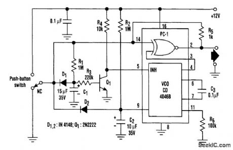
When the switch is in its normally closed (NC) position, capacitors C1 and C2 are held discharged by diodes Dl and D2. Switching off transistor Q1 inhibits the voltage-controlled oscillator of the PLL. The two inputs and, hence, the output of the EX-OR gate (phase comparator 1) ofthe PLL remain at the logic 0 level.When the pushbutton is pressed, C1 and C2 are allowed to charge via resistors R1 and R2. The VCO is enabled only after a time delay (≈0.5 second) set by R1, R3, and C1. During this delay period, the EX-OR gate output follows the logic level at the switch output. As a result, one-shot pulses can be generated by pressing the pushbutton, then releasing it within 0.5 second. R5 provides the switch-debouncing function.If the pushbutton is pressed for more than 0.5 second, the VCO is enabled. The rising voltage at the control input (pin 9) causes a linear increase in VCO frequency and thus accelerates the step-per motor. Releasing the pushbutton discharges C1 and C2 and inhibits the VCO. (View)
View full Circuit Diagram | Comments | Reading(1670)
| Pages:1349/2234 At 2013411342134313441345134613471348134913501351135213531354135513561357135813591360Under 20 |
Circuit Categories
power supply circuit
Amplifier Circuit
Basic Circuit
LED and Light Circuit
Sensor Circuit
Signal Processing
Electrical Equipment Circuit
Control Circuit
Remote Control Circuit
A/D-D/A Converter Circuit
Audio Circuit
Measuring and Test Circuit
Communication Circuit
Computer-Related Circuit
555 Circuit
Automotive Circuit
Repairing Circuit