
Circuit Diagram
Index 1353
Automatic Sprinkling Irrigation Controller (5)
Published:2011/7/14 5:53:00 Author:Sue | Keyword: Automatic, Sprinkling Irrigation, Controller

The 220v ac voltage will generate +12v voltage and +9v voltage after it is reduced by T,rectified by VD1-VD4, stablized by IC1,IC2. The voltages will be provided to the relay K and IC3 respectively.
When to detect soil's humidity, we should stick the humidity detector's two probes into the detected soil(the distance between the two probes are 1-2mm). When the humidity is high, and it reaches the given standard, the resistance value between the humidity detector's two probes is becoming smaller which will make NOT GATE D1's input terminal have high level while the output terminal will have low level. V is disconnected. The relay K doesn't work. The electric motor M doesn't work.
When the soil humidity is becoming low, the resistance value between the humidity detector's two probes is becoming higher which will make NOT GATE D1's input terminal have low level while the output terminal will have high level which will make V connected. K is connected. The electric motor begins to work and the equipment of sprinkler irrigation will begin to work. (View)
View full Circuit Diagram | Comments | Reading(582)
WIEN_BRIDGE_SINE_WAVE_OSCILLATOR
Published:2009/6/24 2:32:00 Author:May

Using the 2N5457 JFET as a voltage vari-able resistor in the amplifier feedback loop, produces a low distortion, constant amplitude sine wave getting the amplifier loop gain just right. The LM103 zener diode provides the voltage reference for the peak sine wave amplitude. (View)
View full Circuit Diagram | Comments | Reading(0)
EASILY_TUNED_SINE_SQUARE_WAVE_OSCILLATORS
Published:2009/6/24 2:31:00 Author:May

This circuit will provide both a sine and square wave output for frequencies from below 20 Hz to above 20 kHz. The frequency of oscillation is easily tuned by varying a single resistor. (View)
View full Circuit Diagram | Comments | Reading(0)
SINE_WAVE_OSCILLATOR
Published:2009/6/24 2:31:00 Author:May

The oscillator delivers a high-purity sinusoid with a stable frequency and amplitude. (View)
View full Circuit Diagram | Comments | Reading(0)
AUDIO_OSCILLATOR
Published:2009/6/24 2:30:00 Author:May

Almost any transistor will work. R1 and C1 will vary the tone. (View)
View full Circuit Diagram | Comments | Reading(0)
Multi Control Switch Circuit Composed of CD4017
Published:2011/7/27 5:37:00 Author:Sue | Keyword: Multi Control, Switch
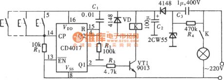
The picture shows the multi control single bond control switch circuit. Usually, we always use bistable flip-flop to compose a switch control circuit which can be on as well as be off. (View)
View full Circuit Diagram | Comments | Reading(724)
CW_IDENTIFIER_WITH_SINE_WAVE_AUDIO_OUTPUT
Published:2009/6/24 2:29:00 Author:May

This identifier can be used to drive a hidden transmitter in a radio fox hunt activity, where the object is to locate a hidden transmitter. (View)
View full Circuit Diagram | Comments | Reading(0)
VERY_LOW_FREOUENCY_GENERATOR
Published:2009/6/24 2:29:00 Author:May

Wien bridge oscillator generates frequen-cies of 1 Hz and 2 to 20 Hz in 2 Hz steps. Maximum output amplitude is 3 volts rms of8.5 volts peak-to-peak. A pot-and-switch at-tenuator allows the output level to be set with a fair degree of precision to any value within a range of 5 decades. (View)
View full Circuit Diagram | Comments | Reading(1070)
Jitter Buffer Switch Circuit Composed of CD4013
Published:2011/7/27 5:38:00 Author:Sue | Keyword: Jitter Buffer, Switch
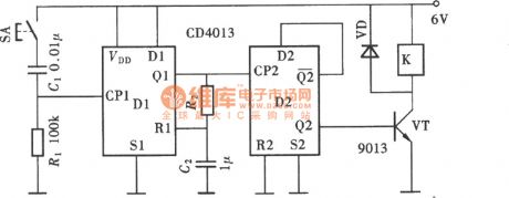
The picture shows the jitter buffer switch circuit composed of CD4013. It uses half of dual D flip-flop to compose bistable control circuit, uses the other half of theflip-flop to compose monostable time delay circuit, and uses one CD4013 to compose a control circuit with complete function. (View)
View full Circuit Diagram | Comments | Reading(4634)
CCFL_SUPPLY_WITH_VARIABLE_CONTRAST
Published:2009/6/24 2:28:00 Author:May

The figure is a complete floating CCFL circuit with variable negative/variable positive-contrast voltage capability, based on the LT1182. Lamp current is programmable from 0 mA to 6 mA using a 0- to 5-V 1-kHz PWM signal at 0% to 90% duty cycle. LCD contrast output voltage polarity is determined by which side of the transformer secondary (either POSCON or NEGCON) the output connector grounds. In either case, LCD contrast output voltage is variable from an absolute value of 10 V to 30 V. The input supply voltage range is 8 V to 28 V. The CCFL converter is optimized for photometric output per watt of input power. CCFL electrical efficiency up to 90% is possible and requires strict attention to detail. LCD contrast efficiency is 82% at full power. (View)
View full Circuit Diagram | Comments | Reading(1489)
WIEN_BRIDGE_OSCILLATOR_2
Published:2009/6/24 2:27:00 Author:May

View full Circuit Diagram | Comments | Reading(530)
WIEN_BRIDGE_OSCILLATOR_1
Published:2009/6/24 2:26:00 Author:May

Wien bridge sine-wave oscillator using two RCA CA3140 op amps covers 30 Hz to 100 kHz with less than 0.5 percent total harmonic distortion. The 10k pot is adjusted for the best waveform. Capacitor C1 and C2 are a two-gang, 450-pF variable with its frame isolated from ground. Maximum output into a 600-ohm load is about 1 volt rms. (View)
View full Circuit Diagram | Comments | Reading(1380)
Sound Controlled Time Delay Energy Saving Switch Circuit Composed of CD4069
Published:2011/7/27 5:38:00 Author:Sue | Keyword: Sound Controlled, Time Delay, Energy Saving
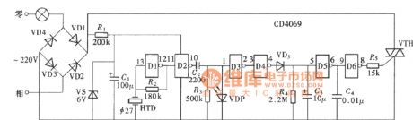
This sound controlled switch has high trigger sensitivity, and it can be triggered by people's footstep and it will close automatically after time delay of 20s. It works well, convenient and energy saving. The circuitconsists ofone hex inverter CD4069, piezoelectric acoustic sensor and one bidirectional thyristor with simple structure. It is economic and convenient with great promotion value. The picture shows the circuit which consists of acoustic sensor, voltage amplifier, light control circuit, delay circuit, thyristor and its trigger circuit. (View)
View full Circuit Diagram | Comments | Reading(903)
Power Supply Circuit of Modem User Interface Circuit
Published:2011/7/22 22:02:00 Author:Michel | Keyword: Modem User Interface, Power Supply Circuit

The above picture is power supply circuit of modem user interface circuit.The circuit consists of single power switch and control integrated circuit etc.It provides the multiple output voltage, power switch can also use N channels MOSFET of low voltage.The input power comes from different output power of AC adapter or the regualted power of parts of the system.UCC3813-5 is power control device and it controls output voltage via contolling VT1 dutyfactor and it provides reference voltage for inverse amplifier of error signal.UCC3813-5 can realize current control mode and the voltage control method.The biggest characteristic of this circuitis to use a control circuit and a MOSFET to provide two telephones voltage. (View)
View full Circuit Diagram | Comments | Reading(1008)
Division Circuit 4(XR-2228)
Published:2011/7/27 5:38:00 Author:Sue | Keyword: Division Circuit
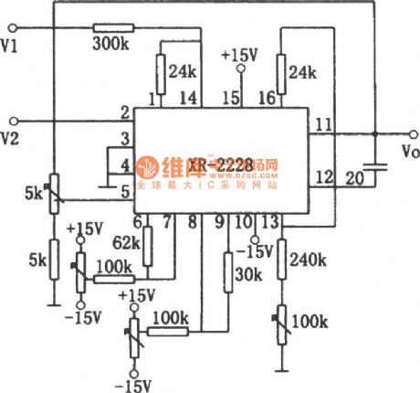
As seen in the figure, the division circuit consists of monolithic multiplier integrated circuit XR-2228. The relation between the output signal V1 and input signal V2 is: Vo=10V1/V2.
The input signal V1 can be either positive or negative but V2 must be negative. If V2 is positive, the circuit will be locked (but it will not broke the integrated package). Every potentiometer is used to adjust the circuit so that it can work at the best working state. At the same time, it can use the known reference voltage to check the circuit. (View)
View full Circuit Diagram | Comments | Reading(639)
ACTIVATE_BACK_UP_POWER_SUPPLY
Published:2009/6/24 2:24:00 Author:May


A circuit,which can be built around two TI TL7702 chips, monitors a 15-V power supply and activates a relay to turn on a back-up supply if the voltage drops below±14.1 V. With the back-up in place, the malfunctioning supply can be replaced without any down time. The TL7702 power-supply voltage supervisor chips are intended for use as reset controllers in microprocessor systems, but they work well in their modified form for this application.One chip detects the positive supply (U1),and the other is used for the negative (U2). A pair of output-relay drive transistors,Q1 and Q2 form a wired OR circuit so that relay K1 is activated by the positive or negative voltalge detector that switches U1 or U2 on.The supervisor chips have a direct connection to the input comparator so that the trigger level is set by a resistor-divider network (R1 and R2) at the sense-input pin.These chip also have an internal, stable, reference-voltage source set at +2.53V,typical.The positive-sensed voltage drops enough to activate the comparator, its output goes low,switches the internal gate,and triggers the siliconcontrolled rectifier (SCR).The output comparator then forces the two output transistors (pin 6) turn on the relay driver,Q1.The negative detector is preceded by halt of the dual op amp LM358N (U3a)-an inverting amplifier with a gain of-0.178.R5 connects to the -15 Vdc being sended. The output of U3a is usually set at 2.67 V, higher than the +2.53-V referenCe voltage. Therefore, no switching occurs. If the -15-Vdc voltage decreases, U2 switihes Q2 and activates K1 in the same manner as described for the U1-Q1 positive detector. R3, R4, and R8 through R10 serve as current-ltmtttng reststois. (View)
View full Circuit Diagram | Comments | Reading(1007)
COMPLEX_SOUND_EFFECT_GENERATOR
Published:2009/6/24 2:38:00 Author:Jessie
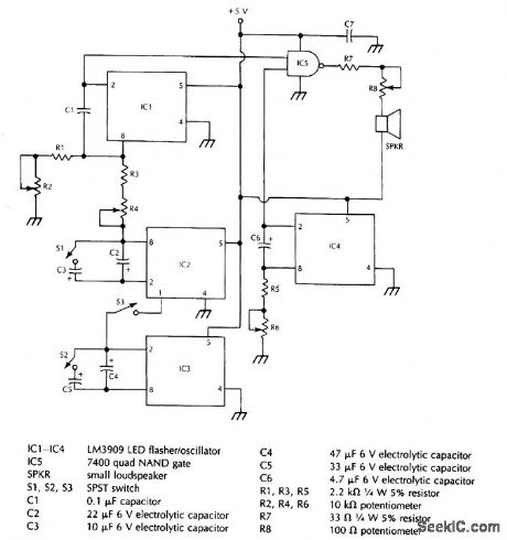
This system uses four free running oscillators to produce a wide variety of complex sounds. LF oscillator IC3 modulates IC2, which modulates IC1. The audio from IC1 is combined with a variable frequency from IC4. Switches at various points allow oscillators IC3 to be switched in or out, IC1 and IC2 to be varied in frequency, and IC4 also can be varied in frequency. The circuit is not critical and different arrangements can be tried to produce various sound effects. (View)
View full Circuit Diagram | Comments | Reading(0)
WIEN_BRIDGE_OSCILLATOR
Published:2009/6/24 2:24:00 Author:May
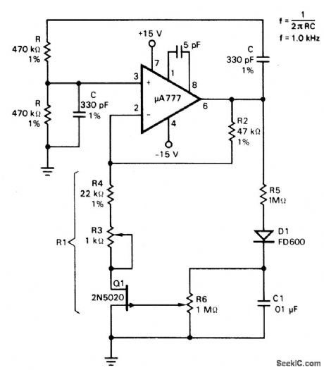
Field effect transistor, Q1, operates in the linear resistive region to provide automatic gain control. Because the attenuation of the RC network is one-third at the zero phase-shift oscillation frequency, the amplifier gain de-termined by resistor R2 and equivalent resis-tor RI must be just equal to three to make up the unity gain positive feedback requirement needed for stable oscillation. Resistors R3 and R4 are set to approximately 1000 ohm less than the required RI resistance. The FET dynami-cally provides the trimming resistance needed to make RI one-half of the resistance of R2. The circuit composed of R5, D1, and C1 iso-lates, rectifies, and filters the output sine wave, converting it into a dc potential to con-trol the gate of the FET. For the low drain-to-source voltages used, the FET provides a symmetrical linear resistance for a given gate-to-source voltage. (View)
View full Circuit Diagram | Comments | Reading(0)
HIGH_EFFICIENCY_TRIPLE_OUTPUT_SUPPLY_FOR_NOTEBOOK_COMPUTERS
Published:2009/6/24 2:37:00 Author:Jessie

The circuit is conftgured to provide output voltages of 3.3 V, 5 V, and 12 V. The current capability of both the 3.3-V and 5-V outputs is 2 A (2.5 A peak). The logic controlled 12-V output can provide 150 mA (200 mA peak), which is ideal for flash memory applications. The operating efficiency shown in the ftgure exceeds 90% for both the 3.3-V and 5-V sections.The 3.3-V section for the circuit in the figure is comprised of the main switch Q4, synchronous switch Q5, inductor L1, and current shunt RSENSE. Current-sense resistor RSENSE monitors the inductor current and is used to set the output current accord-ing to the formula OUT = 100 mV/RSENSE. Advantages of current control include excellent line and load transient rejection, inher-ent short-circuit protection, and controlled start-up currents. Peak inductor currents for L1 and T1 for the circuit in the figure are limited to 150 mV/RSENSE or 3.0 A and 3.75 A, respectively. (View)
View full Circuit Diagram | Comments | Reading(577)
TONE_ENCODER
Published:2009/6/24 2:35:00 Author:Jessie

A basic twin-T circuit uses resistors for accurately setting the frequency of theoutput tones, selected by pushbutton. Momentary switches produce a tone only when the button is depressed. (View)
View full Circuit Diagram | Comments | Reading(2179)
| Pages:1353/2234 At 2013411342134313441345134613471348134913501351135213531354135513561357135813591360Under 20 |
Circuit Categories
power supply circuit
Amplifier Circuit
Basic Circuit
LED and Light Circuit
Sensor Circuit
Signal Processing
Electrical Equipment Circuit
Control Circuit
Remote Control Circuit
A/D-D/A Converter Circuit
Audio Circuit
Measuring and Test Circuit
Communication Circuit
Computer-Related Circuit
555 Circuit
Automotive Circuit
Repairing Circuit