Position: Home > Circuit Diagram > Control Circuit > Jitter Buffer Switch Circuit Composed of CD4013
Control Circuit
Jitter Buffer Switch Circuit Composed of CD4013
Published:2011/7/27 5:38:00 Author:Sue | Keyword: Jitter Buffer, Switch | From:SeekIC

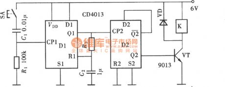
The picture shows the jitter buffer switch circuit composed of CD4013. It uses half of dual D flip-flop to compose bistable control circuit, uses the other half of theflip-flop to compose monostable time delay circuit, and uses one CD4013 to compose a control circuit with complete function.
Reprinted Url Of This Article:
http://www.seekic.com/circuit_diagram/Control_Circuit/Jitter_Buffer_Switch_Circuit_Composed_of_CD4013.html
Print this Page | Comments | Reading(3)

Article Categories
power supply circuit
Amplifier Circuit
Basic Circuit
LED and Light Circuit
Sensor Circuit
Signal Processing
Electrical Equipment Circuit
Control Circuit
Remote Control Circuit
A/D-D/A Converter Circuit
Audio Circuit
Measuring and Test Circuit
Communication Circuit
Computer-Related Circuit
555 Circuit
Automotive Circuit
Repairing Circuit
Code: