
Circuit Diagram
Index 1359
VIDEO_MODULATOR_HOOKUP
Published:2009/6/23 5:06:00 Author:May

This circuit uses an ASTEC UM1683D,but it is typical of many RF video modulators used in VCRs and satellite receivers. (View)
View full Circuit Diagram | Comments | Reading(1672)
WINDOW_COMPARATOR
Published:2009/6/23 5:06:00 Author:May

IC1-c functions as a noninverting compara-tor, and IC1-a operates as an inverting compara-tor. Potentiometer RI and fixed resistors R2 and R3 form a divider chain that delivers slightly dif-ferent voltages to the two comparators. These voltages define the upper and lower limits of the circuit's switching window, which can be changed easily by varying R2 and R3. The LED glows only when the input voltage falls within the window region. (View)
View full Circuit Diagram | Comments | Reading(0)
PRECISION_AUDIO_GENERATOR_FOR_MUSICAL_INSTRUMENT_TUNE_UP
Published:2009/6/23 22:44:00 Author:Jessie

One section of the precision audio frequency generator use an electret microphone element to pick up audio from the piano. That signal is then processed and sent to one channel of a dual-trace oscilloscope. The other section of the circuit is used to produce a variabe-frequency that is fed to a digital frequency counter. After conditioning, the audio signal is presented to the second channel of the scope and output to a set of stereo headphones. (View)
View full Circuit Diagram | Comments | Reading(1435)
LOW_POWER_dc_DOUBLER
Published:2009/6/23 5:02:00 Author:May

This dc voltage-doubler circuit based on the 555 can produce a dc output voltage equal to ap-proximately 2× the dc supply voltage. (View)
View full Circuit Diagram | Comments | Reading(1862)
FREE_RUNNING_MULTIVIBRATOR_USING_OP_AMP
Published:2009/6/23 22:36:00 Author:Jessie
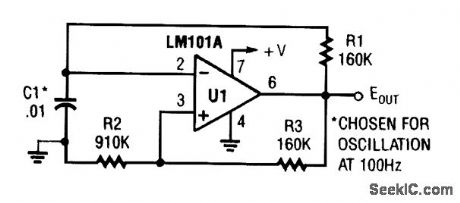
View full Circuit Diagram | Comments | Reading(638)
LINEARAMAMPLITUDE_MODULATOR
Published:2009/6/23 5:01:00 Author:May
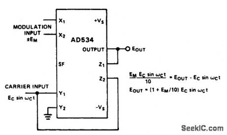
This is a very simple amplitude modulator. It makes use of the Z2 terminal to add the carrier directly to the output, thus bypassing the multi-plier for zero modulation input. It has the advan-tage of allowing operation from a differential modulation input. (View)
View full Circuit Diagram | Comments | Reading(577)
FLIP_FLOP_OR_BISTABLE_MULTIVIBRATOR_WITH_PUSHBUTTON_TRIGGERING
Published:2009/6/23 22:35:00 Author:Jessie
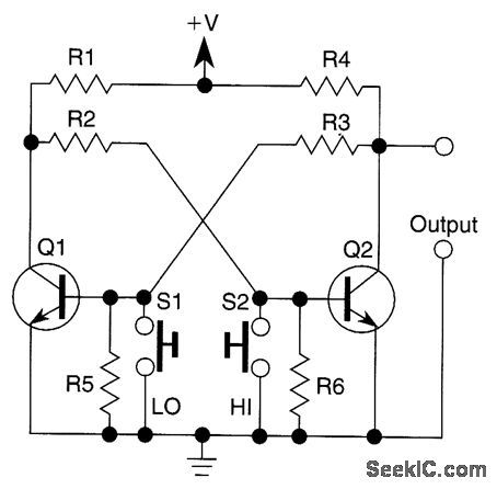
View full Circuit Diagram | Comments | Reading(532)
LOW_POWER_dc_QUADRUPLER
Published:2009/6/23 5:01:00 Author:May

This dc voltage-quadrupler circuit based on the 555 can produce a dc output voltage equal to ap-proximately 4×the dc supply voltage. (View)
View full Circuit Diagram | Comments | Reading(2869)
PULSE_WIDTH_MODULATOR
Published:2009/6/23 5:00:00 Author:May

View full Circuit Diagram | Comments | Reading(1)
LOW_POWER_dc_TRIPLER
Published:2009/6/23 5:00:00 Author:May

This dc voltage-tripler circuit based on the 555 can produce proximately 3× the dc supply voltage. (View)
View full Circuit Diagram | Comments | Reading(4030)
FOUR_QUADRANT_MULTIPLIER_AS_DSB_MODULATOR
Published:2009/6/23 4:57:00 Author:May

View full Circuit Diagram | Comments | Reading(635)
DIGITAL_PULSE_WIDTH_MODULATION_CIRCUIT
Published:2009/6/23 4:54:00 Author:May

This circuit incorporates low-power Schottky transistor/tr ansistor-lo gic (TTL) devices in critical high-speed parts. The 5-MHz clock signal is converted to a 1-MHz signal by a 7490 decade counter configured to divide by 5. The 1-MHz signal is sent, via a clock synchronizer, to a three-stage binary divider that consists of three cascaded 74LS161 binary dividers. The synchronizer consists of a 74LS74 D flip-flop, a 7404 inverter gate, and a 7402 NOR gate. The dividers are programmed from the STD bus by means of three 7475 quad latches; this makes it possible to program the frequency divi-sion from 1 to 4096 (12 bits).The 1-MHz signal is also divided by 1000 by use of three cascaded 7490 decade counters, each configured to divide by 10; this provides a 1-kHz signal, which is sent to a 54121 monostable multivi-brator configured to provide a 0.1-ps pulse, bombarded with an ion beam source in preparation for the materials about to be deposited. While the surface is bombarded with an ion beam, an electron beam source is activated so that a layer of fused silica is vapor-deposited to a total desired thickness value (typically, 1 micron or t0,000 A). The layer offused silica serves as a surface stabilization layer for the next step.A metal mask with an aperture in the specified pattern of the sensor film is placed on the surface at the specified sensor location. The surface area exposed through the mask is cleaned by ion-beam bombardment for a predetermined time. Then as the bombardment continues, a metal (typically, nickel, platinum, and/or palladium) is vapor-deposited through the mask from the electron-beam source to form the sensor film. Deposition is continued until the thickness of the film reaches the value specified in the particular sensor design. A representative value for a nickel sensor film is 2500 A.Next, a pattern for thin film leads is defined by taping directly on the surface of the model with Kapton (or equivalent) polyimide tape. The thin film leads are fabricated by a combination of ion-beam bombardment and electron-beam vapor deposition like that used to deposit the sensor film.The metal vapor deposited in this step is typically copper, gold, or aluminum. A typical thickness for copper leads on the nickel sensor film is about 10,000 A. (View)
View full Circuit Diagram | Comments | Reading(2850)
ASTABLE_MULTIVIBRATOR_Ⅱ
Published:2009/6/23 22:33:00 Author:Jessie

An astable multivibrator based on the 555 is shown. Freq is approximately 975 Hz as determined by the values of RB and C. (View)
View full Circuit Diagram | Comments | Reading(493)
5_A_CONSTANT_VOLTAGE_SUPPLY
Published:2009/6/23 4:51:00 Author:May

This constant-voltage supply has a variable output.It can supply more than 5 A, and has two switchable current limits. (View)
View full Circuit Diagram | Comments | Reading(774)
TELEPRINTER_LOOP_SUPPLY
Published:2009/6/23 4:50:00 Author:May
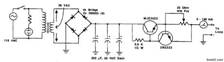
A circuit to power a teleprinter, using transistors as current-controlling devices. The power supply used provides a constant current in a loop, normally 60mA or 20 mA, depending on the machine. (View)
View full Circuit Diagram | Comments | Reading(547)
MONOSTABLE_MULTIVIBRATOR_II
Published:2009/6/23 22:31:00 Author:Jessie
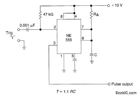
The time constant of RAXC deterrrtines the period of the monostable multivibrator. A negative pulse at pin 2 of the 555 starts the cycle. (View)
View full Circuit Diagram | Comments | Reading(643)
ASTABLE_MULTIVIBRATOR_I
Published:2009/6/23 22:30:00 Author:Jessie
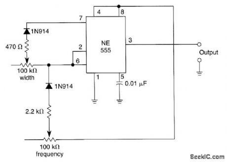
In this multivibrator circuit frequency and pulse width can be separately controlled by using steering diodes (1N914) and two potentiometers. (View)
View full Circuit Diagram | Comments | Reading(1054)
Working principle circuit diagram of RS trigger
Published:2011/7/29 2:39:00 Author:Ecco | Keyword: Working principle , RS trigger
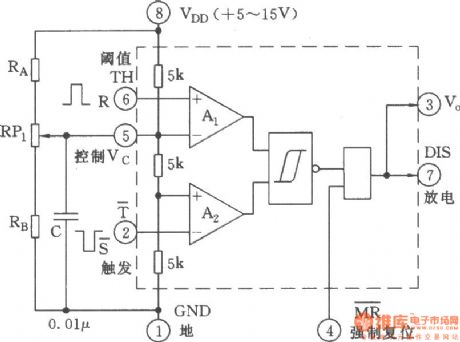
Figure shows the connection diagram,in which 555 is used as RS flip-flop. If removing the control voltage of control end of pin 5, adding a negative, positive control pulse to pin 2, pin 6 respectively, it will form a RS trigger circuit while 555 does not need any external components. R is the reset to control pin 6 of input terminal, also known as the threshold terminal (TH); S is the setting end to control pin 2 of input terminal, that is setting trigger T side. The interior of the output side (pin 3)is actually a push-pull output, so the low output is only 0.3V, high level closes to VDD, it has a strong load capacity; discharge end (pin 7) is the collector open (OC) or open-drain (OD) output. (View)
View full Circuit Diagram | Comments | Reading(1396)
555 long time delay circuit 1
Published:2011/7/29 2:40:00 Author:Ecco | Keyword: 555, long time, delay circuit

As the figure 6-1 shown, the long time delay circuit uses 555 as the core,it usesa high-impedance op-amp CA3140 buffer amplifier, the feedback bootstrap circuit to maintain a constant charging current, to ensure the accuracy of linear and time of charge voltage.
When the pin 2 of 555 is triggered by the low level or the switch is closed to ground, the 555 sets, pin 3 is in high level, so that one of the four analog switches CC4066 S1 is conducted, S2 turns off, C1 charges through R3, R4. The bootstrap circuit produced by feedback op amp keeps the voltage when the both ends of the high-resistance R1 in the charging process. It ensures a linear charging. The current flowing R4 the charging circuit is about 10mA.
CA3140(IC2) is a high-gain low-drift op amp, it is usedas buffer amplifier, the feedback forms the bootstrap circuit. The S4 is mandatory reset switch.
(View)
View full Circuit Diagram | Comments | Reading(1459)
IMPROVED_CMOS_MULTIVIBRATOR
Published:2009/6/23 22:23:00 Author:Jessie
This circuit uses a protective resistor R2 in conjunction with feedback resistor R1. Together, they form a voltage divider to reduce the input voltage amplitude for IC1-a so that the protective diodes never conduct. This improves temperature and voltage stability of the multivibrator. (View)
View full Circuit Diagram | Comments | Reading(648)
| Pages:1359/2234 At 2013411342134313441345134613471348134913501351135213531354135513561357135813591360Under 20 |
Circuit Categories
power supply circuit
Amplifier Circuit
Basic Circuit
LED and Light Circuit
Sensor Circuit
Signal Processing
Electrical Equipment Circuit
Control Circuit
Remote Control Circuit
A/D-D/A Converter Circuit
Audio Circuit
Measuring and Test Circuit
Communication Circuit
Computer-Related Circuit
555 Circuit
Automotive Circuit
Repairing Circuit