
Circuit Diagram
Index 1350
LOW_COST_20_W_AUDIO_AMPLIFIER
Published:2009/6/24 2:59:00 Author:May

This simple inexpensive audio amplifier can be constructed using a couple of TO-220 monolithic Darlington transistors for the push-pull output stage. Frequency response is flat within t dB from 30 Hz to 200 kHz with typical harmonic distortion below 0.2%. The amplifier requires only 1.2 Vrms, for a full 20 W output into an 8 ohm load. Only one other transistor is needed, the TO-92 low-noise high-gain 2N5961 (Q1), to provide voltage gain for driving the output Darlingtons. Its base (point B) is the tie point for ac and dc feedback as well as for the signal input. Input resistance is 10 K. The center voltage at point A is set by adjusting resistor R4. A bootstrap circuit boosts the collector supply voltage of Q1 (point C) to ensure sufficient drive voltage for 6)2. This also provides constant voltage across R7, which therefore acts as a current source and, together with diodes Dl-D3, reduces low-signal crossover distortion. (View)
View full Circuit Diagram | Comments | Reading(2395)
ADJUSTABLE_POSITIVE_REGULATOR
Published:2009/6/24 2:57:00 Author:May

View full Circuit Diagram | Comments | Reading(0)
_GENERAL_PURPOSE_0_TO_30_V_POWER_SUPPLY__
Published:2009/6/24 2:56:00 Author:May

View full Circuit Diagram | Comments | Reading(679)
UP_DOWN_STAIRCASE_WAVE_GENERATOR
Published:2009/6/24 2:56:00 Author:May

This staircase waveform first steps up and then steps down by the circuit shown. An input pulse generator provides the pulses that cause the output to step up or down, depending on the conduc-tion of the clamp transistor, Q1. When this is ON, the down current pulse is diverted to ground and the staircase then steps up. When the upper voltage trip point of Amp 2 is reached, Q1 goes OFF and as a result of the smaller down input resistor (one-half the value of the up resistor, R1), the staircase steps down to the low-voltage trip point of Amp 2. The output voltage, therefore, steps up and down between the trip voltages of the Schmitt Trigger. (View)
View full Circuit Diagram | Comments | Reading(2651)
NONINVERTING_AMPLIFIER_USING_SINGLE_SUPPLY
Published:2009/6/24 3:02:00 Author:Jessie
View full Circuit Diagram | Comments | Reading(624)
FAST_COMPOSITE_AMPLIFIER
Published:2009/6/24 3:01:00 Author:Jessie
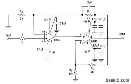
An ultra-low-noise, low-distortion op amp-the AD797-is combined with the AD811 op amp, which offers a high bandwidth and a 100-mA output drive capability. The composite-amplifier circuit serves quite well when driving high resolution ADC's and ATE systems.
The fast AD811 operates at twice the gain of the AD797 so that the slower amplifier need only slew one-half of the total output swing. Using the component values shown, the circuit is capable of better than -90 dB THD with a ±5-V, 500-kHz output signal. If a 100-kHz sine-wave input is used, the circuit will drive a 600-Ω load to a level of 7 V rms with less than -109 dB THD, as well as a 10-kΩ load at less than -117 dB THD.
The device can be modified to supply an overall gain of 5 by changing both the Rf/Rin ratio and R3/R2 ratio to 4: 1. This raises the gains of AD811 and the total circuit while maintaining the AD797 at unity gain. If only the Rf/Rin ratio is changed, the circuit might become unstable. In contrast, if only the R3/R2 ratio is varied, the AD797 will then operate at gain. Subsequently, the circuit will have a lower overall bandwidth. R1 should be equal to the parallel combination of Rin and Rf. (View)
View full Circuit Diagram | Comments | Reading(3398)
WIEN_BRIDGE_SINE_WAVE_OSCILLATOR_1
Published:2009/6/24 2:56:00 Author:May
View full Circuit Diagram | Comments | Reading(792)
BRIDGE_AMPLIFIER
Published:2009/6/24 3:01:00 Author:Jessie
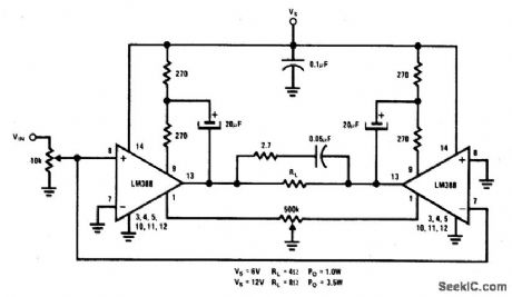
This circuit is for low voltage applications requiring high power outputs. Output power levels of 1.0 W into 4 ohm from 6 V and 3.5 V into 8 ohm from 12 V are typical. Coupling capacitors are not necessary since the output dc levels will be within a few tenths o f a volt of each other. Where critical matching is required the 500 K potentiometer is added and adjusted for zero dc current flow through the load. (View)
View full Circuit Diagram | Comments | Reading(1391)
WIEN_BRIDGE_OSCILLATOR_3
Published:2009/6/24 2:55:00 Author:May

View full Circuit Diagram | Comments | Reading(1739)
MOTOR_DIRECTION_CONTROL_USING_DISCRETE_TRANSISTORS
Published:2009/6/24 3:01:00 Author:Jessie

For best operation, mount the transistors on heatsinks. The transistors specified are fine for small hobby motors, or up to about 6 volts dc and between 800 and 1000 rnA. M1 is a srnall hobby motor. (View)
View full Circuit Diagram | Comments | Reading(1542)
FREE_RUNNING_STAIRCASE_WAVE_GENERATOR
Published:2009/6/24 2:55:00 Author:May
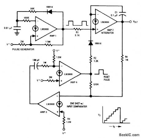
This free-running staircase generator uses all four of the amplifiers, which are available in one LM3900 package. Amp 1 provides the input pulses that pump up the staircase via resistor R1. Amp 2 does the integrate and hold function and also supplies the output staircase waveform. Amps 3 and 4 provide both a compare and a one-shot multivibrator function. Resistor R4 is used to sample the staircase output voltage and to compare it with the power supply voltage (V+) via R3. When the out-put exceeds approximately 80% of V+ the connection of Amps 3 and 4 causes a 100-ps reset pulse to be generated. This is coupled to the integrator (AMP2) via R2 and causes the staircase output voltage to fall to approximately 0 V. The next pulse out of Amp 1 then starts a new stepping cycle. (View)
View full Circuit Diagram | Comments | Reading(2023)
75_WATT_AUDIO_AMPLIFIER_WITH_LOAD_LINE_PROTECTION
Published:2009/6/24 3:00:00 Author:Jessie

View full Circuit Diagram | Comments | Reading(1013)
WIDE_RANGE_OSCILLATOR_FREQUENCY_RANGE_OF_5000_TO_1
Published:2009/6/24 2:54:00 Author:May

Timing resistor R may be adjusted to any value between 10 K and 50 M to obtain a fre-quency range from 400 kHz to 100 Hz. Return-ing the timing resistor to the collector of Q1 ensures that Q1 draws its base current only from the timing capacitor Ct. The timing capacitor recharges when the transistors are off, to a voltage equal to the base emitter volt-age of Q2 plus the base emitter drops ofQ1 and Q2. The transistors then start into conduction. Capacitor Cs is used to speed up the transition. A suitable value would be in the region of 100 pF. (View)
View full Circuit Diagram | Comments | Reading(1003)
STEPPER_MOTOR_ENCODER_CIRCUIT
Published:2009/6/24 3:00:00 Author:Jessie

This circuit translates shaft rotation and direction to a readout on an LED display. A stepper motor is used as an encoder. (View)
View full Circuit Diagram | Comments | Reading(3602)
VIDEO_STAIRCASE_GENERATOR
Published:2009/6/24 2:54:00 Author:May
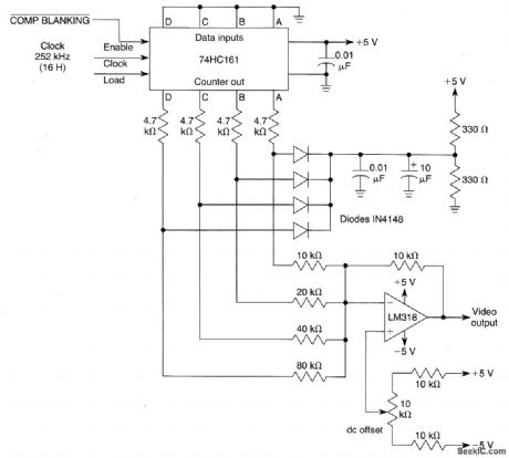
Using a 74HC161 counter and a simple D-A converter using an op amp and resistor network, a very simple video staircase generator for gray-scale generation (12 bars) can be obtained. The out-put is clean and mostly free of glitches. (View)
View full Circuit Diagram | Comments | Reading(1499)
TUNABLE_SINGLE_COMPARATOR_OSCILLATOR
Published:2009/6/24 2:53:00 Author:May
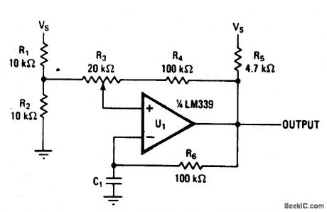
Varying the amount of this comparator circuit's hysteresis makes it possible to vary output frequencies in the 740-Hz to 2.7-kHz range smoothly. The amount of hysteresis to-gether with time constant R6C1 determines how much time it takes for C1 to charge or discharge to the new threshold after the output voltage switches. (View)
View full Circuit Diagram | Comments | Reading(1112)
ADJUSTABLE_BIAS_REGULATOR
Published:2009/6/24 2:59:00 Author:Jessie


If the wiper of R2 is set at N% rotation,the bias voltage Will be∶This method derives a bias voltage that tracks VBE of this bias transistor. If the bias transistor is thermally linked to the power stage, tracking over a wide temperature range will result. (View)
View full Circuit Diagram | Comments | Reading(1289)
STEPPER_MOTOR_AS_SHAFT_ENCODER
Published:2009/6/24 2:59:00 Author:Jessie

To use a stepper as a shaft encoder, the out-put signals must be converted to square waves with a pair of voltage comparators. (View)
View full Circuit Diagram | Comments | Reading(2408)
STEPPER_MOTOR_PULSE_GENERATOR
Published:2009/6/24 2:59:00 Author:Jessie
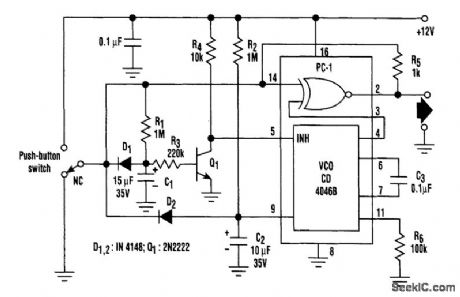
When the switch is in its normally closed (NC) position, capacitors C1 and C2 are held discharged by diodes Dl and D2. Switching off transistor Q1 inhibits the voltage-controlled oscillator of the PLL. The two inputs and, hence, the output of the EX-OR gate (phase comparator 1) ofthe PLL remain at the logic 0 level.When the pushbutton is pressed, C1 and C2 are allowed to charge via resistors R1 and R2. The VCO is enabled only after a time delay (≈0.5 second) set by R1, R3, and C1. During this delay period, the EX-OR gate output follows the logic level at the switch output. As a result, one-shot pulses can be generated by pressing the pushbutton, then releasing it within 0.5 second. R5 provides the switch-debouncing function.If the pushbutton is pressed for more than 0.5 second, the VCO is enabled. The rising voltage at the control input (pin 9) causes a linear increase in VCO frequency and thus accelerates the step-per motor. Releasing the pushbutton discharges C1 and C2 and inhibits the VCO. (View)
View full Circuit Diagram | Comments | Reading(0)
LOW_COST_20_W_AUDIO_AMPLIFIER
Published:2009/6/24 2:59:00 Author:Jessie
This simple inexpensive audio amplifier can be constructed using a couple of TO-220 monolithic Darlington transistors for the push-pull output stage. Frequency response is flat within t dB from 30 Hz to 200 kHz with typical harmonic distortion below 0.2%. The amplifier requires only 1.2 Vrms, for a full 20 W output into an 8 ohm load. Only one other transistor is needed, the TO-92 low-noise high-gain 2N5961 (Q1), to provide voltage gain for driving the output Darlingtons. Its base (point B) is the tie point for ac and dc feedback as well as for the signal input. Input resistance is 10 K. The center voltage at point A is set by adjusting resistor R4. A bootstrap circuit boosts the collector supply voltage of Q1 (point C) to ensure sufficient drive voltage for 6)2. This also provides constant voltage across R7, which therefore acts as a current source and, together with diodes Dl-D3, reduces low-signal crossover distortion. (View)
View full Circuit Diagram | Comments | Reading(0)
| Pages:1350/2234 At 2013411342134313441345134613471348134913501351135213531354135513561357135813591360Under 20 |
Circuit Categories
power supply circuit
Amplifier Circuit
Basic Circuit
LED and Light Circuit
Sensor Circuit
Signal Processing
Electrical Equipment Circuit
Control Circuit
Remote Control Circuit
A/D-D/A Converter Circuit
Audio Circuit
Measuring and Test Circuit
Communication Circuit
Computer-Related Circuit
555 Circuit
Automotive Circuit
Repairing Circuit