
Circuit Diagram
Index 1341
TEMPERATURE_CONTROLLER
Published:2009/6/24 3:51:00 Author:May
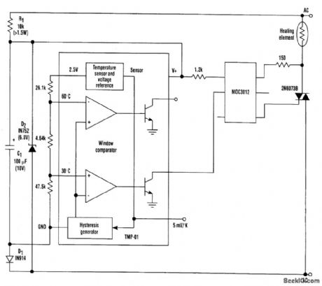
The temperature sensor/controller (the TMP-01) is a monolithic device whose low power allows it to operate with a simple half-wave rectified power supply directly from the ac line. Such an ar-rangement greatly simplifies the power-supply design requirement to the point of only needing a few low-cost components to provide a single +6-Vdc supply.The TMP-01 is essentially a therrrtostat on a chip. It includes a linear temperature sensor (5 mV/K), and also has two comparators that switch at externally determined set points. These set points are established by resistively dividing the internal 2.5-V reference to set appropriate voltages on the inputs to the comparators.One comparator is used in this circuit to turn on the heating element when the temperature drops below 30℃; it corresponds to a voltage of 1.52V on the comparator's input. (View)
View full Circuit Diagram | Comments | Reading(0)
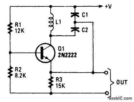
COLPITTS_OSCILLATOR
Published:2009/6/24 4:07:00 Author:Jessie
View full Circuit Diagram | Comments | Reading(1)
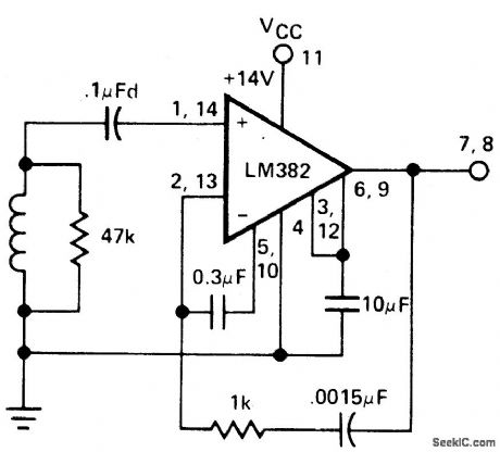
MAGNETIC_PHONO_PREAMPLIFIER
Published:2009/6/24 3:51:00 Author:May

View full Circuit Diagram | Comments | Reading(765)
118_TO_136_MHz_AIRCRAFT_RECEIVER
Published:2009/6/24 3:50:00 Author:May

This recelver covers the 118-to 136-MHz AM aviation band It has a 10 7-MHz IF amplifier. L1,L3,and L5 are 1 1/2 turns of#24wire FIL1 is a 10 7-MHz ceramic filter.IF bandwidth will be about 250 kHz. (View)
View full Circuit Diagram | Comments | Reading(2447)
COURTESY_LIGHT_EXTENDER
Published:2009/6/24 4:07:00 Author:Jessie
Most car door switches are simply single-pole switches, with one side grounded. When the door is opened the switch grounds the other line thus completing the light circuit. In a car where the negative terminal of the battery is connected to the chassis, the,.g,J tive wire of the unit (emitter of Q2) is con-nected to chassis the positive wire (case of 2N3055) is connected to the wire going to the switch. 1n a car having a positive ground sys-tem this connection sequenge is reversed. When the switch closes (door open), C1 is discharged via D1 to zero volts, and when the switch opens, g| charges up via R1 and R2.Transistors Q1 and Q2 are connected as an emitter follower (Q2 just buffers Q1) therefore the voltage across Q2 increases slowly as Ci charges. Hence Q2 acts like a low resistance in parallel with the switch and keeps the lights on.The value of C1 is chosen such that a usetui light level is obtained for about four seconds; therefore the light decreases until in about 10 seconds it is out completely. With different transistor gains and with variation in current drain due to a particular type of car, the timing may vary but may be simply adjusted by selecting C1. (View)
View full Circuit Diagram | Comments | Reading(0)
TAPE_RECORDING_AMPLIFIER
Published:2009/6/24 3:49:00 Author:May

View full Circuit Diagram | Comments | Reading(609)
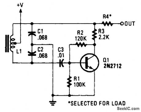
LC_AUDIO_OSCILLATOR
Published:2009/6/24 4:06:00 Author:Jessie
View full Circuit Diagram | Comments | Reading(1376)
ASTABLE_MULTIVIBRATOR
Published:2009/6/24 3:49:00 Author:May


View full Circuit Diagram | Comments | Reading(0)
NE602_LOCAL_OSCILLATOR_CIRCUITS
Published:2009/6/24 4:05:00 Author:Jessie
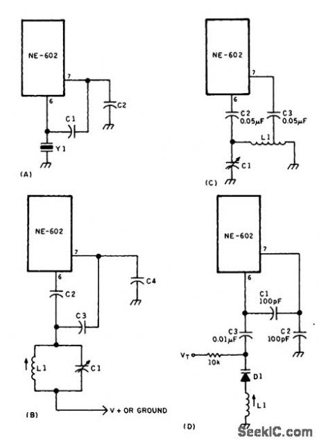
Local oscillator circuits for the NE602. (View)
View full Circuit Diagram | Comments | Reading(0)
TAPE_PREAMPLIFIER_NAB_EQUALIZATION
Published:2009/6/24 3:49:00 Author:May
View full Circuit Diagram | Comments | Reading(506)
NATIONAL_SEMICONDUCTOR
Published:2009/6/24 4:05:00 Author:Jessie
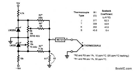
A circuit for use with grounded thermocouples is shown. To trim, short out the LM329B and ad-just R5 so that V°= αT, where cc is the Seebeck coefficient of the thermocouple and T is the absolute temperature. Remove the short and adjust R4 so that W equals the thermocouple output voltage at ambient. A good grounding system is essential here, for any ground differential will appear in series with the thermocouple output. (View)
View full Circuit Diagram | Comments | Reading(1552)
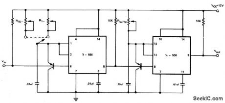
UNIVERSAL_WIPER_DELAY
Published:2009/6/24 4:04:00 Author:Jessie

IC1 is connected in the astable mode, driving RLA. C3, Dl, and D2 prevent spikes from the relay coil and the wiper motor from triggering IC1. VR2 is adjusted to give the minimum delay time required. VR1 is the main delay control and provides a range of from about 1 second to 20 seconds. SW1 is an over-ride switch to hold RLA permanently on (for normal wiper operation). The relay should have a resistance of at least 150 ohms and have heavy duty contacts. The suppression circuit may be needed for the protection of IC1. (View)
View full Circuit Diagram | Comments | Reading(1934)
OPERATING_WAVEFORMS
Published:2009/6/24 4:03:00 Author:Jessie

View full Circuit Diagram | Comments | Reading(860)
EIGHT_INPUT_A_D_CONVERTER_FOR_TEMPERATURE_MEASUREMENTS
Published:2009/6/24 4:03:00 Author:Jessie


The actual processing circuitry of this A/D converter consists of only four parts: U2, U3, R1 and R2. Eight temperature probes are used with the circuit; however, they can be replaced with other types of sensors, as long as resistors R3 through R10 are removed.
(View)
View full Circuit Diagram | Comments | Reading(4084)
SPEED_WARNING_DEVICE
Published:2009/6/24 4:03:00 Author:Jessie
View full Circuit Diagram | Comments | Reading(0)
FLAT_RESONSE_AMPLIFIER_FIXED_GAIN_CONFIGURATION
Published:2009/6/24 3:55:00 Author:Jessie
View full Circuit Diagram | Comments | Reading(476)
OPTICAL_SAFETY_CIRCUIT_SWITCHES
Published:2009/6/24 3:55:00 Author:Jessie
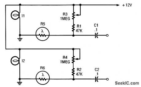
Use of two LDR devices replaces the two vide light sources for the LDR devices. (View)
View full Circuit Diagram | Comments | Reading(465)
PREAMPLIFIER_WITH_RIAA_NAB_COMPENSATION
Published:2009/6/24 3:54:00 Author:Jessie
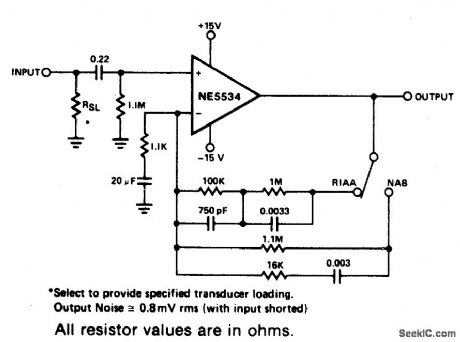
View full Circuit Diagram | Comments | Reading(1117)
OPTOISOLATOR_AND_OPTOCOUPLER_INTERFACE_CIRCUITS
Published:2009/6/24 3:51:00 Author:Jessie
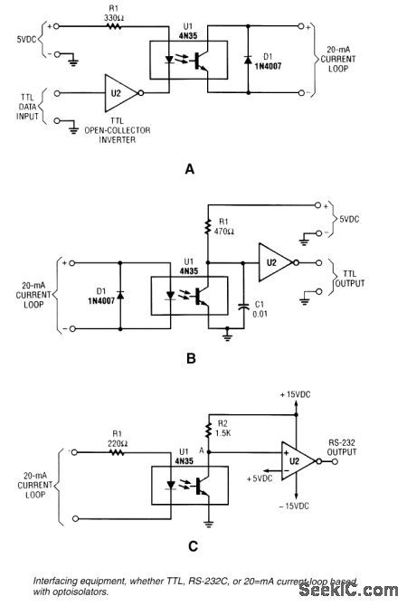

A circuit for isolating a variable resistor is shown. An optoisolator that has an LED and a photo-conductive cell (or photoresistor) is used. The current through the LED controls its brightness, which in turn determines the resistance between terminals A and B. The LED current is set by the voltage of the dc power supply and the value of the two resistors (R1 and R2). The fixed resistor (R1) is used to limit the current to a maximum of 20 mA (when the resistance of the potentiometer, R2, is set to zero ohms), otherwise, the LED might burn out. (View)
View full Circuit Diagram | Comments | Reading(3381)
OPTOCOUPLER_CIRCUITS
Published:2009/6/24 3:52:00 Author:Jessie
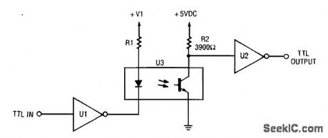
This circuit is a TTL-to-TTL isolator circuit. The driver circuit is an open-collector TTL inverter (U1). When the input is high, then the output of the inverter is low. Thus, when the input is high, the output of U1 grounds the cathode end of the LED and causes the LED to turn on. (View)
View full Circuit Diagram | Comments | Reading(1146)
| Pages:1341/2234 At 2013411342134313441345134613471348134913501351135213531354135513561357135813591360Under 20 |
Circuit Categories
power supply circuit
Amplifier Circuit
Basic Circuit
LED and Light Circuit
Sensor Circuit
Signal Processing
Electrical Equipment Circuit
Control Circuit
Remote Control Circuit
A/D-D/A Converter Circuit
Audio Circuit
Measuring and Test Circuit
Communication Circuit
Computer-Related Circuit
555 Circuit
Automotive Circuit
Repairing Circuit