555 Circuit
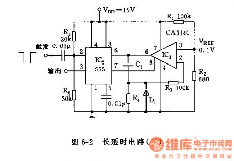
555 long time delay circuit 2
Published:2011/7/29 2:23:00 Author:Ecco | Keyword: 555, long time , delay circuit | From:SeekIC


The circuit is shown as the chart 6-2, the delay circuit is a trigger delay circuit with integrator.
CA3140 is a BIMOS single-supply op amp, itcan still work when the value ofVref is very low or zero, and its gate (pin 8)can discharge frompin 7of 555 (through D1). Diode D1is required to the J-FET gate - source PN junction with smaller leakage, the conduction current is high, reverse leakage is small (about 100pA).
As shown in Figure 5-2, the delay circuit is a trigger delay circuit with integrator. When the negative pulse is triggered, the pin 3 is in high level, and pin 7 is in open circuit, then C2R4 integrator makes line integralon the reference voltage Vref = 0.1V divided by the R1, R2.
Reprinted Url Of This Article:
http://www.seekic.com/circuit_diagram/555_Circuit/555_long_time_delay_circuit_2.html
Print this Page | Comments | Reading(3)

Article Categories
power supply circuit
Amplifier Circuit
Basic Circuit
LED and Light Circuit
Sensor Circuit
Signal Processing
Electrical Equipment Circuit
Control Circuit
Remote Control Circuit
A/D-D/A Converter Circuit
Audio Circuit
Measuring and Test Circuit
Communication Circuit
Computer-Related Circuit
555 Circuit
Automotive Circuit
Repairing Circuit
Code: