
Circuit Diagram
Index 1150
12_V_buck_boost_from_a_45_V_to_15_V_input
Published:2009/7/24 2:25:00 Author:Jessie

Figure 7-55 shows the MAX1771 connected to provide a 12-V output at 250 mA, with a 4.5-V to 15-V input. See Fig. 7-51 for component suppliers. MAXIM NEW RELEASES DATA Book, 1995, P. 4-26. (View)
View full Circuit Diagram | Comments | Reading(1375)
RANDOM_SIGNAL_GENERATOR
Published:2009/7/24 2:24:00 Author:Jessie

Signals arise from fluctuations in dense layer of positive ions near cathode of 2D21 grid-controlled gas-discharge tube. Used with computers to simulate random action, such as effect of wind gusts on controls of airplane.-N. D, Diamantides and C. E. McCray, Generating Random Forcing Functions for Control System Simulation, Electronics, 34:33, p 60-63. (View)
View full Circuit Diagram | Comments | Reading(1139)
20_40_CPS_VARIABLE_SWEEP
Published:2009/7/24 2:23:00 Author:Jessie

Used to lest servos and related equipment. Sawtooth waveform developed by unijunction transistor circuit is used to key blocking oscillator.-M. Rosen, Subaudio Swapt Signal Generator, Electronics, 33:17, p 67-68. (View)
View full Circuit Diagram | Comments | Reading(668)
PHOTOELECTRIC_WELD_MONITOR
Published:2009/7/24 2:23:00 Author:Jessie

Shuts off r-f generator automatically after copper lows when welding exhaust tubulation to metal vacuum tube. Light is refected by molten copper into phototube that initiates shutdown, with 0.6 sec delay introduced intentionally to allow copper to low around entire seal.-J. Markus and V. Zeluff, Handbook of Industrial Electronic Control Circuits, McGraw-Hill, New York, 1956, p 344. (View)
View full Circuit Diagram | Comments | Reading(1046)
AC_MOTOR_CONTROL
Published:2009/7/2 4:19:00 Author:May

The circuit illustrates feedback speed regulation of a standard ac induction motor, a function difficult to accomplish other than with a costly, generator type, precision tachometer. When the apertured disc attached to the motor shaft allows the light beam to cross the interrupter module, the programmable unijunction transistor, Q1, discharges capacitor, C1, into the much larger storage capacitor, C2. The voltage on C2 is a direct function of the rotational speed of the motor. Subsequently, this speed-related potential is compared against an adjustable reference voltage, V1, through the monolithic operational amplifier, A1, whose output, in turn, establishes a dc control input to the second P.U.T.(Q2). This latter device is synchronized to the ac supply frequency and furnishes trigger pulses in the conventional manner to the triac at a phase angle determined by the speed control, R1, and by the actual speed of the motor. (View)
View full Circuit Diagram | Comments | Reading(3017)
Differential_sensing_for_the_type_K_thermocouple
Published:2009/7/24 2:23:00 Author:Jessie

Fig. 13-16 This circuit combines full-differential sensing and filtering for a type-K thermocouple. The circuit has 120-dB dc common-mode rejection if all signals remain within the LTC1043 supply-voltage range. The LTC switched-capacitor building block transfers charge between the input flying capacitor and the output capacitor. The LTC1043 commutating frequency, which is settable, controls the rate of charge (and hence the overall bandwidth). The differential inputs reject noise and common-mode voltages (within the LTC1043 supply range). Excursions outside these limits require protection networks, as shown in Fig. 13-16B. As in Fig. 13-15, the optional pull-down resistor permits negative readings. The 1-MΩ resistor provides a bias path for the LTC1043 floating inputs. Linear Technology. Linear Applications Handbook 1990 p AN28-6. (View)
View full Circuit Diagram | Comments | Reading(876)
PIERCE_TETRODE_TRANSISTOR
Published:2009/7/24 2:23:00 Author:Jessie

Tuned to third overtone of crystal fundamental. Fifth harmonic of oscillator is used as calibration frequency for c-w receiver of radio direction linden-A. T. Lloyd, Direction Finder Helps Recover Discoverer Capsule, Electronics, 34:9, p 42-45. (View)
View full Circuit Diagram | Comments | Reading(731)
500_MHz_075_W_amplifier_28-V_supply
Published:2009/7/24 2:22:00 Author:Jessie
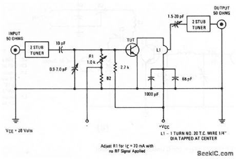
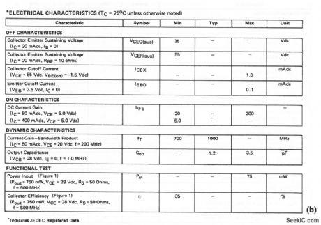
The electrical characteristics for the 2N4428 shown in this circuit are given in Fig.2-17B. (View)
View full Circuit Diagram | Comments | Reading(671)
VHF_SWEPI_OSCILLATOR
Published:2009/7/24 2:22:00 Author:Jessie
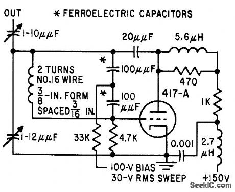
Voltage-tunable ferroelectric capacitors give tuning ratio of about 2 to 1 from 20 to 250 Mc and 1.5 to 1 from 250 to 400 Mc.-T. W. Butler, Jt., Ferroelectrics Tune Electronic Circuits, Electronics, 32:3, p 52-55. (View)
View full Circuit Diagram | Comments | Reading(577)
Step_up_down_for_5_V_33_V_output
Published:2009/7/24 2:22:00 Author:Jessie

Figure 7-54 shows the MAX1771 connected to provide either 5-V or 3.3-V output at 0.5 A, with a 3-V to 11-V input. See Fig. 7-51 for component suppliers. MAXIM NEW RELEASES DATA Book, 1995, P. 4-25. (View)
View full Circuit Diagram | Comments | Reading(762)
VARIABLE_HYSTERESlS_SCHMITT
Published:2009/7/2 4:18:00 Author:May
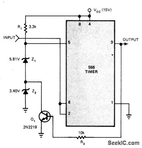
Uses standard 555 timer with only five additional components to give fully TTL/DTL-compatible Schmitt trigger that responds to slow input ramps as well as straight DC levels. When input is 0, output goes high and tums on Q1. When input increases to 5.8 V, output goes low and Q1, tums off. Decreasing output to 4.7 V (lower threshold point) makes output high again. For values shown, hysteresis is thus 1.1 V. Threshold points and hysteresis value can be adjusted as required by changing zeners used.-M. K.Lalitha and P. R. Chetty, Variable-Threshold Schmitt Trigger Uses 555 Timer, EDN Magazine, Sept. 20, 1976, p 112 and 114. (View)
View full Circuit Diagram | Comments | Reading(685)
ELECTRONIC_CROSSOVER_CIRCUIT
Published:2009/7/2 4:18:00 Author:May
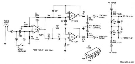
An audio source, such as a mixer, preamplifier, equalizer, or recorder, is fed to the Electronic Crossover Circuit's input. That signal is either ac- or dc-coupled, depending on the setting of switch 51, to the non-inverting input of buffer-amplifter U1a, one section of a quad, BIFET, low-noise TL074 op amp made by Texas Instruments. That stage has a gain of 2, and its output is distributed to both a lowpass filter made by R4, R5, C2, C3, and op-amp Uld, and a highpass filter made by R6, R7, C4, C5, and op amp Ulc. Those are 12 dB/octave Butterworth-type filters. The Butterworth filter response was chosen because it gives the best compromise between damping and phase shift. Values of capacitors and resistors will vary with the selected crossover at which your unit will operate. The filter's outputs are fed to a balancing network made by R8, R9, R10, R11 and balance potentiometer R14. When the potentiometer is at its mid-position, there is unity gain for the passbands of both the high and low filters. Dc power for the Electronic Crossover Circuit is regulated by R12, R13, D1, and D2, and decoupled by C6 and C7. (View)
View full Circuit Diagram | Comments | Reading(3977)
LOW_PASS_DIGITAL_FILTER
Published:2009/7/2 4:15:00 Author:May

Used to retrieve pulse train data from noisy signal line. Filtering is achieved with SN7400 quad two-input NAND gate, SN7413 dual four-input Schmitt trigger, two diodes, and two capacitors. One gate of SN7400 is used as inverter driving pulse delay operating on negative-going transition of input pignal. Other Schmitt trigger, diode, and capacitor provide delay on positive-going transition. Any additional pulses occurring during delaycirouit time-out resets delay time without affecting output.-T. H. Haydon. Low-Pass Digital Filter. EDN Magazine. Nov. 20. 1973. p 85. (View)
View full Circuit Diagram | Comments | Reading(1826)
SLIDING_TONE_DOORBELL
Published:2009/7/2 4:14:00 Author:May
When the doorbell is pushed, you'll hear a low tone that will slide up to a higher frequency. The frequency of the AF oscillator is determined by coupling capacitor, C1 and the value of the resistance connected between the base of Q1 and ground. That resistance, RBG is equal to (R1 + R2) R3. First, assume that 51 is closed and R2 has been adjusted td produce a pleasant, low-frequency tone. Capacitor C3 will charge through R6 until it reaches such a voltage that it will cause diode D1 to conduct. When that happens, the value of RBG is paralleled by R4, Thus, because the total resistance RBG decrease, the output tone slides up in frequency. Capacitor C3 will continue to charge until the voltage across D2 and D3 causes those diodes to conduct. Then RBG is paralleled also by R5, the total resistance again decreases, and the oscillator's frequency again increases. (View)
View full Circuit Diagram | Comments | Reading(604)
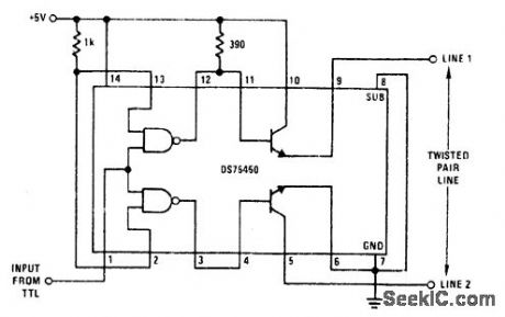
BALANCED_LINE_DRlVER
Published:2009/7/2 4:13:00 Author:May

National DS75450 dual peripheral driver serves as interface between TTL and twisted-pair line. Output line 1 is terminated to ground through haff of line impedance, and line 2 is terminated to +5 V through half of line impedance. Output current is 300 mA.- Interface Databook, National Semiconductor, Santa Clara, CA, 1978, p 3-20-3-30. (View)
View full Circuit Diagram | Comments | Reading(602)
ELECTRONIC_BELL
Published:2009/7/2 4:12:00 Author:May
Coarse frequency is controlled by the capacitors which must be kept nearly identical in value to each other for best results. Fine tuning is accomplished with R1 and R2. The decay time is controlled by R3. (View)
View full Circuit Diagram | Comments | Reading(1271)
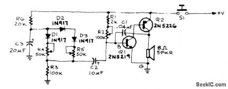
LOU_COST_CHIME_CIRCUIT
Published:2009/7/2 4:11:00 Author:May
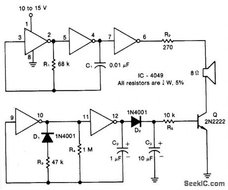
Resistor R1, capacitor C1, and two inverters form a square wave generator, which produces the basic tone. The generator is followed by an inverter that acts as both a buffer and a driver for the speaker. Resistor R2, which has a minimum value of 100 ohms, limits the current and controls the volume. Diode D1, ca-pacitor C2, resistors R3 and R4, and two inverters create the pulse generator that determines the turn-on and decay times of the chime. The decay circuit-formed by D2, C3, R5, and Q-reduces the amplitude of the chime tone exponentially as a function of time. (View)
View full Circuit Diagram | Comments | Reading(695)
DUAL_OUTPUT_I_F
Published:2009/7/24 3:10:00 Author:Jessie
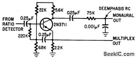
Final i-f stage of stereo f-m set has two outputs, to permit independent feed of monaural f-m.-S. Messin and T. E. Nawalinski, A Solid State Stereo Set Built in Modules, Electronics, 38:16, p 88-92 (View)
View full Circuit Diagram | Comments | Reading(770)
CMOS_INTERFACE_FOR_OPAMP
Published:2009/7/2 4:08:00 Author:May
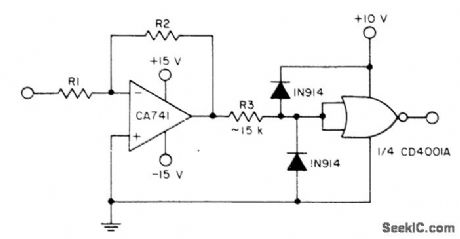
Clamp diodes and single resistor provide interface between CMOS circuit and opamp operating between normal ±15 V supply rails. Diodes ensure that CMOS input voltage does not go outside permissible range.- COS/MOS Integrated Circults, RCA Solid State Division,Somerville,NJ,1977,p 629 (View)
View full Circuit Diagram | Comments | Reading(534)
PREAMP_MODULE
Published:2009/7/24 3:09:00 Author:Jessie
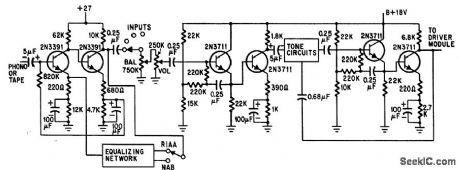
Bootstrapped emitter-followers accept high-impedance input signals and minimize loading of equalizing and tone circuits.-S. Messin and T. E. Nawalinski, A Solid State Stereo Set Built in Modules, Electronics, 38:16, p 88-92. (View)
View full Circuit Diagram | Comments | Reading(953)
| Pages:1150/2234 At 2011411142114311441145114611471148114911501151115211531154115511561157115811591160Under 20 |
Circuit Categories
power supply circuit
Amplifier Circuit
Basic Circuit
LED and Light Circuit
Sensor Circuit
Signal Processing
Electrical Equipment Circuit
Control Circuit
Remote Control Circuit
A/D-D/A Converter Circuit
Audio Circuit
Measuring and Test Circuit
Communication Circuit
Computer-Related Circuit
555 Circuit
Automotive Circuit
Repairing Circuit