
Circuit Diagram
Index 1156
THREE_DIMENSIONAL_TARGET_SIMULATOR
Published:2009/7/24 2:34:00 Author:Jessie

Trigger generator supplies zero time reference for ppi and rhi scopes and circuits of radar simulator. Course generator provides voltages proportional to X, Y, and Z target coordinates. Transformation computer with function generators converts these into polar coordinates. Range voltage from computer is compared with linear sawtooth to obtain time delay proportional to target range.-J. I. Leskinen, Four Ways lo Simulate Radar Targets, Electronics, 31:23, p 82-86. (View)
View full Circuit Diagram | Comments | Reading(601)
RAZOR_SHARP_CW_FILTER
Published:2009/7/2 2:57:00 Author:May

The circuit consists of four stages of active bandpass ftltering provided by two typeμA747 integrated-circuit dual op amps and includes a simple threshold detector (diodes D1 and D2) between stages 2 and 3 to reduce low-level background noise. Each of the four filter stages acts as a narrow bandpass ftlter with an audio bandpass centered at 750 Hz. The actual measured 3-dB bandwidth is only 80 Hz wide. (View)
View full Circuit Diagram | Comments | Reading(1961)
FIBER_OPTIC_RECEIVER
Published:2009/7/2 2:55:00 Author:May
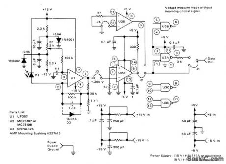
Uses MFOD100 PIN photodiode as optical detector for handling megabit data rates. Minimum photocurrent required to drive LF357 opamp U1 is 250 nA, Voltage comparator U2 inverts output of U1 and provides standard TTL output. For CMOS output, quad two-input NAND gate U3 is wired into circuit, with jumper J1 connected from U3 output to output terminal of receiver. Adjust R1 to give accurate reproduction of 1-MHz square wave with 50% duty cycle at receiver output.- Basic Experimental Fiber Optic Systems, Motorola, Phoenix, AZ, 1978. (View)
View full Circuit Diagram | Comments | Reading(0)
DIGITALLT_TUNED_LOW_POWER_ACTIVE_FILTER
Published:2009/7/2 2:53:00 Author:May

This constant gain, constant Q, variable frequency filter provides simultaneous low-pass, bandpass, and high-pass outputs with the component values shown, the center frequency will be 235 Hz and 23.5 Hz for high and low logic inputs respectively; Q = 100, and gain = 100. (View)
View full Circuit Diagram | Comments | Reading(753)
5_V_SUPPLY_INCLUDING_STABILIZED_MOMENTARY_BACKUP
Published:2009/7/2 2:50:00 Author:May

Circuit Notes
This circuit protects microprocessor systems from“brownouts”without the expense of an uninterruptible power supply. Designed around a small 9-V nickel cadmium battery the circuit continues to provide a constant 5-V output during brownouts of up to a few seconds, Load currents of up to 500 mA may be drawn using the components shown.With this mains-derived supply present, D5 is forward biased so that the stabilized sup-ply powers the 5-V regulator and hence the circuitry to be protected. FET Ty is held on by D1, its drain current being provided from the dc supply via Rb and D2. Diode D3 is reverse-biased so that T2 is off, and the battery is isolated from D6. RCH and D4 serve to trickle charge the battery with approximately 1.2 mA.When the 12-V supply is removed, RI and C1 initially keep T1 switched on. D3 is now forward biased, so that T1 drain current is drawn via Rb, D3 and T2 from the battery. This switches T2 on, allowing the load circuitry to draw current from the battery via D6 and the 5-V regulator. After a few seconds C1 has discharged (via RI) such that Vgs falls below thq threshold value for the FET, and T1 switches off. There is then no path for T2 base current, so that it also switches off, isolating the battery. (View)
View full Circuit Diagram | Comments | Reading(589)
ACTIVE_LOW_PASS_FILTER_WITH_DIGITALLY_SELECTED_BREAK_FREQUENCY
Published:2009/7/2 2:50:00 Author:May


Variable low-pass ftlter has break frequencies at1, 10, 100 Hz and 1 kHz. The break frequency isThe low frequency gain isA second break frequency(a zero)is introduced by rDS(on )of the DG201A,causing theminimum gain to bea maximum attenuation of 40 dB (80 dB relative to the low frequency gain)。 (View)
View full Circuit Diagram | Comments | Reading(824)
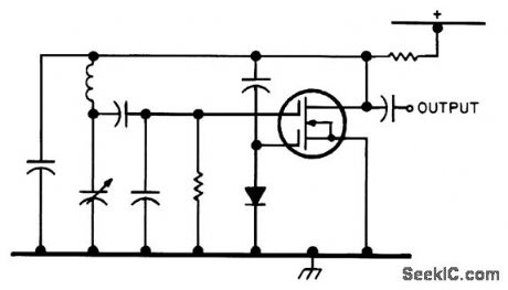
STABLE_HF_VFO
Published:2009/7/24 2:34:00 Author:Jessie

This circuit is a Hartley oscillator, as identified by the fact that the feedback to the JFET transistor (Q1) is supplied by a tap on the tuning inductance (L1). The position of the tap is usually between 10 and 35 percent of the total coil length. A buffer amplifier is included, and it provides two basic functions: It boosts the low output power from the oscillator to a higher level and it isolates the oscillator from changing load impedances. The main tuning capacitor (C1) is a 100-pF air-dielectric variable unit of heavy-duty double-bearing construction, The trimmer (C2) is used to set the exact frequency, especially when using a dial that must be calibrated. Note that several of the fixed capacitors are indicated as being NPO ceramic-disk, polystyrene, or silvered mica (in order of preference). Also notice that a voltage regulator (U1) serves the oscillator. This generates very little heat; nonetheless, it is still a good idea to mount the regulator away from the actual oscillator circuit. The small trimmer capacitors (C2 and C4) are air-dielectric types, rather than mica or ceramic. The purpose of C4 is to provide dc blocking to the transistor-gate circuit. It has such a small value because we want to lightly load the LC-tuned circuit. That trimmer is adjusted from a position of minimum capacitance (i.e., with the rotor plates completely unmeshed from the stator plates), and is then advanced to a higher capacitance as the oscillator is turned on and off. The correct position is the lowest value that allows the oscillator to start immediately every time that power is applied.
(View)
View full Circuit Diagram | Comments | Reading(3320)
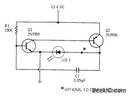
NOISE_GENERATOR
Published:2009/7/2 2:42:00 Author:May
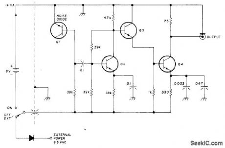
Used with communication receiver to measure Q of tuned circuit without disconnecting circuit. Noise diode gives constant noise signal strength over wide frequency band. so frequency response of tuned circuit can be observed with receiver. Q is calculated after using S-meter of receiver to find -6 dB bandwidth. AII transistors are 2N2368; select noisiest for Q1. Article covers test setup for measuring Q.-R. C. Marshall. Q Measure-ment and More. Ham Fladio. Jan. 1977. p 49-51. (View)
View full Circuit Diagram | Comments | Reading(564)
0-5000_Hz_WHITE_NOlSE
Published:2009/7/2 2:30:00 Author:May
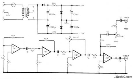
Both signal and noise levels are continuously and independently variable from zero to maximum in simple noise generator developed to demonstrate recovery of low-level 500.Hz signal from noise. Circuit gives maximum noise output into 1500-ohm load; for lower load impedances, reduce noise level to prevent oscillation. Opamps require±15 V supply.Which can be simple voltage doubler with regulation,-J.E.Morris.Simple Noise Generator.Wireless world.April 1977.p 62. (View)
View full Circuit Diagram | Comments | Reading(717)
WIDEBAND_TWO_POLE_HIGH_PASS_FILTER
Published:2009/7/2 2:26:00 Author:May

The circuit provides a 10MHz cutoff frequency.Resistor R3 ensures that the tnputcapacitance of the amplifier does not interact with the filter response at the frequencyof interest.An equivalent low pass filter is similarly obtained by capacitance and resistance transformation (View)
View full Circuit Diagram | Comments | Reading(0)
LOW_COST_UNIVERSAL_ACTIVE_FILTER
Published:2009/7/2 2:18:00 Author:May


The circuit as shown in Fig. 1 gives the bandpass operation the transfer function calculated from
Interchanging the capacitor C with the resistor R at the input of the circuit high-pass operation is obtained. A low-pass filter is obtained by applying two parallel connections of R and C as shown in Fig. 2.
The low-pass operation may be much improvedwith the circuit as gtven h Fig.3.Here the gamand Q may be set up separately with respectto the cut-off frequency according to theequations (View)
View full Circuit Diagram | Comments | Reading(847)
LIGHT_TRANSMISSION_CHECKER
Published:2009/7/2 2:16:00 Author:May
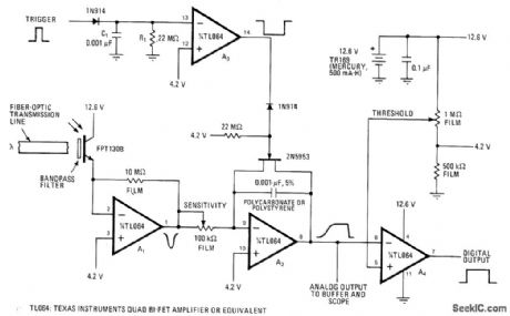
Phototransistor and quad opamp serve as total-energy detector of pulsed-light signals propagated through fiber-optic cable of communication system. Can be used for checking and comparing condition of long fibers if light intensity of source is held constant. Will also detect changes in light intensity and changes in pulse width. Circuit gives linear response to light levels from 100 to 10,000 ergs/cm2 if minimum pulse width is at least10 μs. A2, acts as RC integrator, giving voltage proportional to total light energy received. A4 provides comparison to fixed level.-E. W. Rummel, Low-Level-Light Detector Checks Optical Cables Fast, Electron-Jcs, April 27, 1978, p 148 and 150.
(View)
View full Circuit Diagram | Comments | Reading(1246)
IF_NOISE_BLANKER
Published:2009/7/2 2:15:00 Author:May
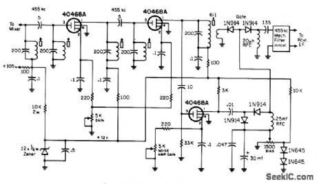
Used ahead of 455.kHz IF strip of communication receiver to provide about 40-dB attenuation of ignition and other noise pulses that can interfere with reception in 2- and 6-meter amateur bands. Two paths for noise pulses, one AC and the other DC, must be balanced for good operation. Resistor and capadtor values in noise rectifier are chosen to select sharp noise pulses in preference to signals. DC noise pulses are amplified by pulse amplifier and converted to AC notse pulses. Settings of pots are optimized for best noise blanking. Circuit requires 12-V supply, which can be obtained from receiver with appropriate dropping resistors and zener as shown for +105 V, or from separate source.-F. C. Uones. Ex. perimental I.F. Noise Blankers, CQ, March 1971, p81-83. (View)
View full Circuit Diagram | Comments | Reading(2365)
NEURON_SIMULATOR
Published:2009/7/24 2:39:00 Author:Jessie


Simulates many of functions of eye and ear nerve cells. Output consists of 6.Mc pulses.-Artificial Neuron Uses Transistors, Electronics, 32:7, p 74. (View)
View full Circuit Diagram | Comments | Reading(1059)
LF_OR_HF_FIELD_STRENGTH_METER
Published:2009/7/2 2:14:00 Author:May

C1 and L1 resonate on the 1750 meter band, with coverage from 150 kHz to 500 kHz. L1 can be slug-tuned for 160-to-190 kHz coverage alone or a 2.5 mH choke can be used for L1, if desired, using C1 for tuning. A 1N270 germanium diode rectifies the RE signal and C2 is charged at the peak RF level. This dc level is amplified by an LM358.The gain is determined by R2 and R3, 1 100-kilohm linear potentiometer that varies the dc gain from 1 to 100, driving the 50 microampere meter. This field strength meter need not be limited to LF use. The Table shows the L1 and C1 values for HF operation and broadband operation. (View)
View full Circuit Diagram | Comments | Reading(1511)
Platinum_RTD_signal_conditioner_with_curvature_correction
Published:2009/7/24 2:39:00 Author:Jessie

Fig.13-23 This simple circuit provides an accuracy of 0.25℃ over 2℃ to 400℃ sensed range, Note that one side of sensor Rp is grounded to minimize noise problems. To calibrate, substitute a precision decade box(General Radio 1432)for Rp. Set the box to the 5℃ value(1019.9Ω)and adjust the 5℃ trim for 0.05 V at the LT1006. Next, set the box for the 400℃ value(2599.9Ω)and adjust the 400℃ trim for a 4.000-V output, Repeat this procedure until both points are fixed. The resistance values given are for a nominal 1000.0-Ω(0℃)sensor. Sensors that deviate from this nominal value can be used by factoring In the deviation from 1000.0Ω Linear Technology. Linear Application Handbook 1990, AN23-1. (View)
View full Circuit Diagram | Comments | Reading(783)
VFO_AGC_CIRCUIT
Published:2009/7/24 2:39:00 Author:Jessie
This is a possible simple AGC system for use with a Vackar oscillator, which should be an improvement over a diode connected directly between gate and source. D1 can be any good-quality RF silicon diode. (View)
View full Circuit Diagram | Comments | Reading(1058)
SPEECH_SIMULATOR
Published:2009/7/24 2:38:00 Author:Jessie
Electron-coupled 1-kc Colpitts oscillator is modified to hunt at approximately 10 cps. Serves as source of fluctuating-amplitude audio lone, to simulate speech in narrow spectrum region.-H. Schwarzlander, Intelligibility Evaluation of Voice Communications, Electronics, 32:22, p 88-91. (View)
View full Circuit Diagram | Comments | Reading(541)
500_MHz_20_mW_oscillator_10_V_supply
Published:2009/7/24 2:38:00 Author:Jessie
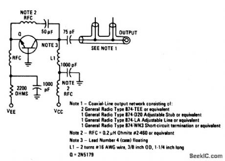
The electrical characteristics for the 2N5179 shown in this circuit are given in Fig.2-24B. (View)
View full Circuit Diagram | Comments | Reading(810)
FIBER_OPTIC_TRANSMTTER
Published:2009/7/2 2:13:00 Author:May
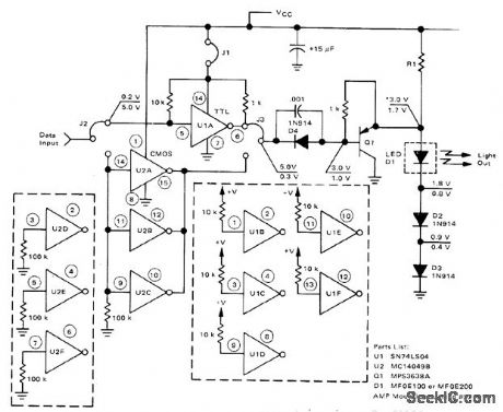
Will handle NRZ data rates to 10 megabits or square waves to 5MHz。 Input is rrL- or CMOS-compatible depending on circuit selected.Transmitter drawsonly 150 mA from 5-V supply for TTL or from 5-15 V supply for CMOS Choose RI to glve LED drive current for proper operation of system For TTL operation,jumpers J1,J2,and J3 are connected as shown. For CMOS operation, remove J1 and transfer J2 and J3 to altemate positions for connecting to U2. Choice of LED depends on system length and desired data rate.Power supply can be HP6218A or equivalent. DC voltages shown are for TTL interface, with uppervaluefor LED on at 50 mA and lowervalue for LED off.- Basic Experimental Fiber Optic Systems, Motorola, Phoenix, AZ, 1978. (View)
View full Circuit Diagram | Comments | Reading(1243)
| Pages:1156/2234 At 2011411142114311441145114611471148114911501151115211531154115511561157115811591160Under 20 |
Circuit Categories
power supply circuit
Amplifier Circuit
Basic Circuit
LED and Light Circuit
Sensor Circuit
Signal Processing
Electrical Equipment Circuit
Control Circuit
Remote Control Circuit
A/D-D/A Converter Circuit
Audio Circuit
Measuring and Test Circuit
Communication Circuit
Computer-Related Circuit
555 Circuit
Automotive Circuit
Repairing Circuit