
Circuit Diagram
Index 1155
THYRISTOR_SPARK_QUENCHER
Published:2009/7/2 3:02:00 Author:May
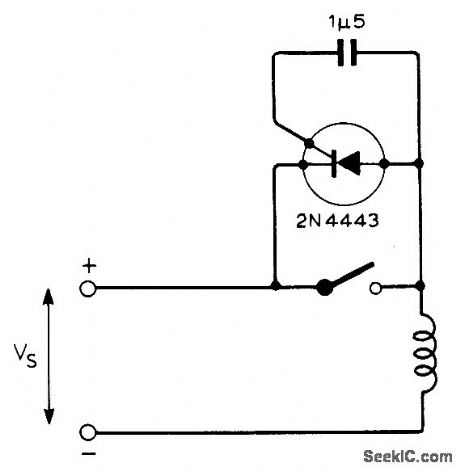
Suppresses arcing at contacts when switching large inductive loads. Use SCR capable of operating at well over twice supply voltage and passing full load current during swhch-off. SCR shown will handle up to 500 V at up to BO A provided current pulses are under 8 ms.-E. Potter. Switch Spark Quench for Inductive Loads. Wireless World. Dec. 1973. p 605. (View)
View full Circuit Diagram | Comments | Reading(833)
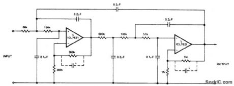
PRECISION,FAST_SETTLING,LOW_PASS_FILTER
Published:2009/7/2 3:02:00 Author:May

This circuit is useful where fast signal acquisition and high precision are required, as in electronic scales. The filter's time constant is set by the 2 K ohm resistor and the 1 μF capacitor until comparator No, 1 switches. The time constant is then set by the 1.5 M ohm resistor and the 1 μF capacitor. Comparator No. 2 provides a quick reset.The circuit settles to a final value three times as fast as a simple 1.5 M ohm-1μF filter, with almost no dc error. (View)
View full Circuit Diagram | Comments | Reading(757)
Oven_temperature_controller
Published:2009/7/24 2:46:00 Author:Jessie


Pig. 13-27 This circuit shows a precision temperature controller for a small-component oven. When power is applied, the thermistor (a negative TC device) is at a high value. A1saturates positive. This forces the LT3525A switching regulator output low, biasing Q1. As the heater warms, the thermistor value decreases. When the inputs balance, A1comes out of saturation and the LT3525A pulse-width modulates the heater via Al, completing a feedback path. The 2-kHz pulse-width-modulated heater power is much faster than the thermal-loop response and the oven sees an even, continuous heat flow. Linear Technology Linear Applications Handbook, 1990, p. AN5-1. (View)
View full Circuit Diagram | Comments | Reading(1756)
PULSED_HORN_ALARM
Published:2009/7/2 3:01:00 Author:May

Two CMOS packages incorporate multiple time delays to improve convenience and effectiveness of auto intrusion alarm. R1C1 gives 30-s delay for arming alarm after it is turned on by switch concealed inside car, to let driver get out of car. R2C2 gives 15-s delay before alarm sounds after door is opened, to allow driver to get back in car again and disable alarm. R3C3 turns off alarm in 300 s and resets alarm system for next intrusion. Car horn is pulsed 60 times per minute, so alarm would not be confused with stuck horn. Article tells how circuit works and gives detailed instruc-tions for instailation and connection to door and trunk switches.-G. Hinkle, Give the Hamburglar Heart Failure, 73Magazine, Feb. 1977, p 36-37. (View)
View full Circuit Diagram | Comments | Reading(858)
-10_V_GIVES_10_kHz
Published:2009/7/2 3:00:00 Author:May

Control voltage input in range of 0 to -10 V is converted linearly to frequency of digital output pulse train haiving fullscale value of 10 kHz. Internal regulation of circuit makes operation essentially independent of ±15 V supply level.A1 is opamp integrator, A2 is comparator, and A3 is precision mono MVBR. Transistor switch Q1 connects Rb to 3.15-V reference voltage during t1 timing period of A3.—W.G.Jung, IC Timer Cookbook, Howard W.Sams, Indianapolis, IN, 1977, p184-192 (View)
View full Circuit Diagram | Comments | Reading(0)
_12_1__and__20_V_dual_supply
Published:2009/7/24 2:41:00 Author:Jessie

Figure 7-62 shows the MAX662A flash-memory supply (Figs. 7-58 through 7-61) used as a dual power supply. Figure 7-63 shows the output-current characteristics. Maxnvt NEW RELEASES DATA Book, 1995, P.4-80. (View)
View full Circuit Diagram | Comments | Reading(527)
RADAR_TARGET_ACCELERATION_SIMULATOR
Published:2009/7/24 2:40:00 Author:Jessie
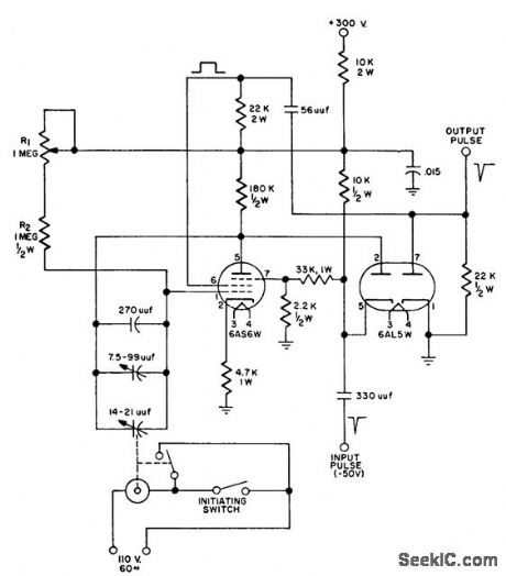
Used for testing radar range tracking systems. Uses phantastron delay modified by adding synchronous. motor. driven capacitor in feedback loop to provide target with con trolled acceleration. Pulse used to trigger phantastron corresponds to radar transmitted pulse; second pulse, triggered by trailing edge of phantastron square-wave, represents radar echo. Time between pulses, representing range, can be set to desired values by changing resistance between positive supply and grid and changing capacitance between plate and grid of phantastron tube.-Radar Target Acceleration Simulator, Electronic Circuit Design Handbook, Mactier Pub. Corp., N.Y., 1965, p 171. (View)
View full Circuit Diagram | Comments | Reading(1350)
50_kHz_FM_OPTICAL_RECEIVER
Published:2009/7/2 3:00:00 Author:May
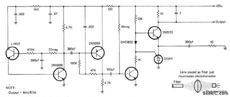
Designed for pulse-rate modulation system in which transmitter varies pulse rate of modulated light beam in optical-fiber cable above and below center frequency of 50 kHz. L14G2 GE photo transistor converts modulated optical light to RF signal for demodulation and reconstruction of original audio. Based on circuit in General Electric Opto-Electronics Manual. -I. Math, Math's Notes, CQ, July 1977, p 67-68 and 90. (View)
View full Circuit Diagram | Comments | Reading(1781)
TEMPERATURE_COMPENSATING_VFO_CIRCUITS
Published:2009/7/24 2:40:00 Author:Jessie

Here are two ways in which adjustable temperature compensation can be achieved: (a) with a differential capacitor, and (b) with two conventional trimmers. (View)
View full Circuit Diagram | Comments | Reading(790)
175_MHz_70_W_amplifier_28_V_supply
Published:2009/7/24 2:39:00 Author:Jessie
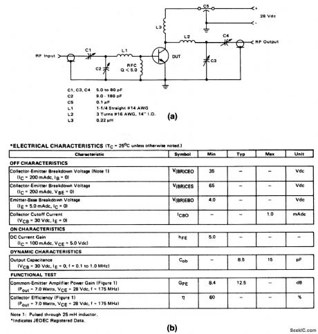
The electrical characteristics for the 2N5641 shown in this circuit are given in Fig. 2-26B. (View)
View full Circuit Diagram | Comments | Reading(1565)
EXCESS_NOISE_SOURCE
Published:2009/7/2 2:21:00 Author:May

Develops about 18 dB of excess noise in region of 50-300 MHz for optimizing converter or receiver for best noise figure. Can also be used for noise optimizing of TV receivers and for peaking UHF TVfront ends. Q1 and Q2 form cross-coupled 7OO-CR1 MVBR. C1 is greater than C2 to favor conduction of Q2. When Q2 is on, Q3 turns on and makes current flow through broadband noisediode CR1. Diode is forward-biased because available gating voltage does not generate enough noise in reversebias mode. If noise output is too great, insert 20000-ohm attenuator as shown.-T. E. Hartson, A Gated Noise Source, QST, Jan. 1977. p 22-23. (View)
View full Circuit Diagram | Comments | Reading(826)
STATE_VARIABLE_FILTER
Published:2009/7/2 2:22:00 Author:May
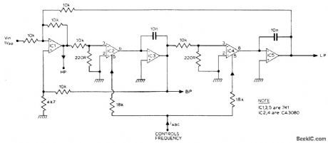
The filter produces three outputs: high-pass, bandpass, and low-pass. Frequency is linearly proportional to the gain of the two integrators. Two CA3080's, (IC2, 4) provide the variable gain, the resonant frequency being proportional to the current IABC. Using 741 op amps for IC3 a control range of 100 to 1, (resonant frequency) can be obtained.If CA3140's are used instead of 741's then this range can be extended to nearly 10,000 to 1. (View)
View full Circuit Diagram | Comments | Reading(1521)
CORE_DRIVER
Published:2009/7/24 2:36:00 Author:Jessie
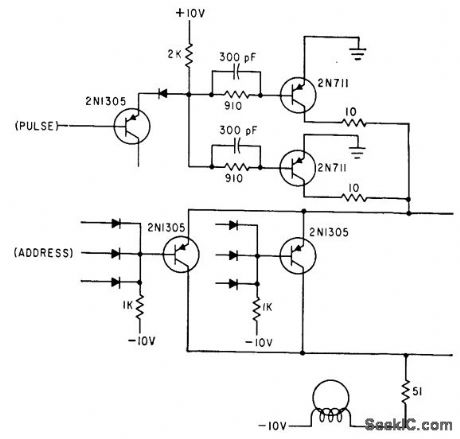
Causes current with fast rise and fall time to flow through steering driver that has been actuated by outputs of address counter used in generating programmed digital signals for simulation or test purposes.-W. D. Woo, Novel Digital Signal Generator Uses Magnetic, Core Pegboard, Electronics, 35:27, p 46-49. (View)
View full Circuit Diagram | Comments | Reading(622)
Alternate_relative_humidity_sensor
Published:2009/7/24 2:35:00 Author:Jessie

Fig. 13-21 This circuit is an alternate to that of Fig. 13-20. The circuit requires two op amps, but only one LTC1043 package. Calibration is the same as for Fig. 13-20. Linear Technology Lineal Applications Handbook 1990 p AN3-8.
(View)
View full Circuit Diagram | Comments | Reading(649)
POWER_SWITCHING_CIRCUIT
Published:2009/7/2 3:00:00 Author:May
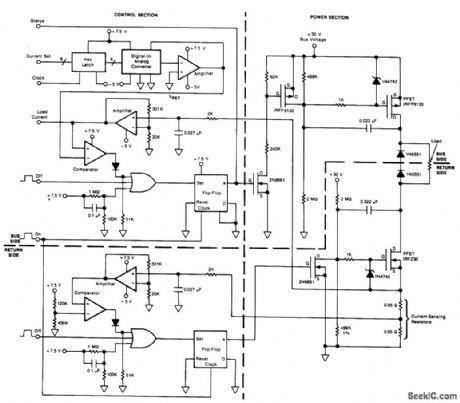
Circuit Notes
This circuit provides on/off switching, soft starting, current monitoring, current tripping, and protection against overcurrent for a 30 Vdc power supply at normal load currents up to 2 A. The switch is turned on by an“on”command pulse; it is turned off by an“off”command pulse. An overcurrent trip can also be set on the bus side by a 6-digit binary signal, which is converted to an analog voltage and compared with the amplified voltage developed across a loadcurrent-sensing resistor. Resistor/capacitor combinations(0.027 μF, 2 kO)at the inputs of the current-sensing amplifiers act as low-pass filters: this introduces a few hundred its of delay in the response to overcurrent, thereby providing some inununity to noise. The 0.022 pF capacitors connected to the drain terminals of the PFETs provide a Miller effect, which reduces the rate of change of the drain voltage and therefore the rate of rise of current at turn-on. The soft-turn-on time depends upon the load impedance and is typically 100 to 200 ms. (View)
View full Circuit Diagram | Comments | Reading(637)
NUCLEAR_BLAST_SIMULATOR
Published:2009/7/24 2:35:00 Author:Jessie
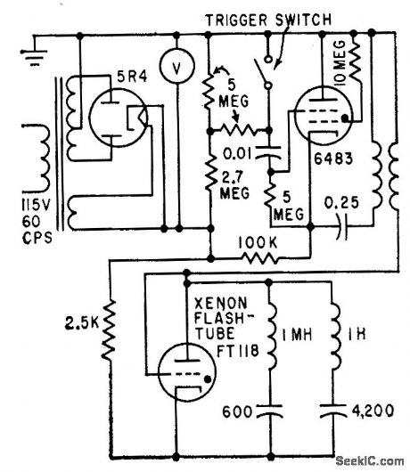
Uses xenon flashtube in double-discharge circuit to simulate thermal radiation pulse of nuclear explosion within atmosphere, which rises rapidly to first maximum, declines to minimum, rises to second maximum, then decreases gradually to zero. Used to evaluate atomic bomb alarm systems.-D. J. Baker and D. E. Thomas, Nuclear Thermal Pulse Simulator, Electronics, 32:44, p 66-69. (View)
View full Circuit Diagram | Comments | Reading(1573)
FIFTH_ORDER_CHEBYSHEV_MULTIPLE_FEEDBACK_LOW_PASS_FILTER
Published:2009/7/2 2:59:00 Author:May
The low bias currents permit high resistance and low capacitance values to be used to achieve low frequency cutoff. fc=10 Hz, Avct =4, Passband ripple = 0.1 dB.Note that small capacitors (25-50 pF) may be needed for stability in some cases. (View)
View full Circuit Diagram | Comments | Reading(550)
LASER_DIODE_SOURCE
Published:2009/7/2 2:57:00 Author:May
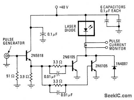
With transistor switching circuit shown for RCA SG2007 laser diode, pulses as short as 10 ns are possible at repetition rates above 100 kHz. Used in optical communication system in which fiber bundle or singlefiber is attached directly to laser pellet.-J. T. O'Brien, Laser Diodes Provide High Power for High-Speed Cornmunieations Systems, Electronics, Aug. 5, 1976, p 94-96. (View)
View full Circuit Diagram | Comments | Reading(1466)
NE602_COLPITTS_VFO
Published:2009/7/24 2:35:00 Author:Jessie
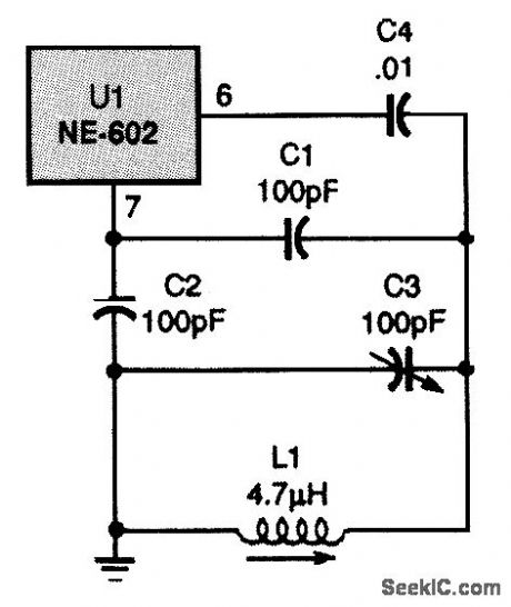
In this Colpitts variable-frequency oscillator (VFO), an inductor/capacitor combination is used to set the frequency. (View)
View full Circuit Diagram | Comments | Reading(1049)
CURRENT_DRAIN_SENSOR
Published:2009/7/2 2:57:00 Author:May
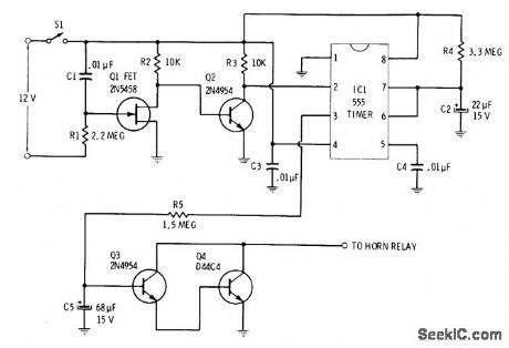
Current drawn bydome light when door is open or by ignition when turned on triggers current-sensing stages Q1 and Q2 to start 555 timer and apply power to horn relay. Initial15-s delay in sounding horn allows owner to enter car and open hidden switch S1 to deactivate alarm. If S1 is not opened during delay interval, horn sounds for about 90 s, then circuit automatically resets itself. C5 and R5 control duration of initial 15-s delay.C2 and R4 control total time that horn sounds.-R. F. Graf and G. J. Whalen, The Build-It Book of Safety Electronics, Howard W. Sams, Indianapolis, IN, 1976, p 57-62. (View)
View full Circuit Diagram | Comments | Reading(1372)
| Pages:1155/2234 At 2011411142114311441145114611471148114911501151115211531154115511561157115811591160Under 20 |
Circuit Categories
power supply circuit
Amplifier Circuit
Basic Circuit
LED and Light Circuit
Sensor Circuit
Signal Processing
Electrical Equipment Circuit
Control Circuit
Remote Control Circuit
A/D-D/A Converter Circuit
Audio Circuit
Measuring and Test Circuit
Communication Circuit
Computer-Related Circuit
555 Circuit
Automotive Circuit
Repairing Circuit