
Circuit Diagram
Index 1157
Flash_memory_programming_supply_30_mA
Published:2009/7/24 2:38:00 Author:Jessie

Figure 7-58 shows a MAX662A connected to provide a +12-V, 30-mA output for programming byte-wide flash memories. Figure 7-59 shows component suppliers. Figures 7-60 and 7-61 show connections for programming commercial-temperature range, and extended /military-range applications, respectively. Quiescent current is 185 μA, with 0.5-μA shutdown current. The IC has a logic-controlled shutdown pin that allows direct microprocessor control. MAXIM NEW RELEASES DATA BOOk, 1995, P. 4-75, 4-79. (View)
View full Circuit Diagram | Comments | Reading(704)
HIGH_CURRENT_INFRARED_LED_PULSER
Published:2009/7/2 2:10:00 Author:May


Circuit operates as regenerative amplifier for delivering 10-μs pulses with amplitude of 1.1 A and repetition rate of 1.4 kHz to infrared LED. Suitable for infrared beacon in fiber-optic communication and optical radar applications. Drain is 100 mA from 10-V supply. Use gallium arsenide LED such as SSL-55C or TIL32 for high-output infrared transmitter. Q2 can be changed to ger manium transistor such as 2N1305 to give peak current of 2 A at pulse width of 15 μs and 750-Hz repetition rate.-F. M Mims, Electronic Circuitbook 5: LED Projects, Howard W. Sams, Indianapolis, IN, 1976, p 33-35. (View)
View full Circuit Diagram | Comments | Reading(1391)
CLUTTER_GENERATOR
Published:2009/7/24 2:38:00 Author:Jessie
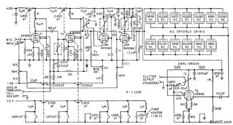
Simulates radar clutter received by rotating antenna on 550-mph aircraft, for checking airborne moving-target indicator on ground. Clutter is produced by ringing bank of closely spaced crystals and allowing resulting frequencies to beat together to produce jagged clutter return that decoys with range.-H. Lobenstein and A. R. Dial, Radar-Return Simulator Tests Moving-Target Indicators, Electronics, 33:49, p 58-60. (View)
View full Circuit Diagram | Comments | Reading(773)
COLPITTS_VFO
Published:2009/7/24 2:37:00 Author:Jessie


Three capacitors (C1, C2, and C3) are used in this NE602AN IC Colpitts oscillator circuit, rather than two, because of the need for dc blocking. The values of the components are as follows:
C1,C2,C3≈2400/ƒ(MHz)C4=1/[(2πƒ)2 L1]L1≈7/ƒ(MHz)microhenries (View)
View full Circuit Diagram | Comments | Reading(1576)
Single_cell_undervoltage_indicator
Published:2009/7/24 2:37:00 Author:Jessie

This circuit is essentially a voltage-controlled multivibrator that causes a red LED (D1) to flash. The flash rate is set by voltage from the single cell (about 1.4 sec-1 for 1.2 V, with a 300-μA drain, and 5.5 sec-1 at 1.55 V, with a 800-μA drain. To get an equivalent visibility with continuous operation would require more than 5-mA drain. (View)
View full Circuit Diagram | Comments | Reading(709)
200_MHz_high_gain_amplifier_6_V_supply
Published:2009/7/24 2:37:00 Author:Jessie

The electrical characteristics for the 2N5179 shown in this circuit are given in Fig.2-24B. (View)
View full Circuit Diagram | Comments | Reading(585)
Linearized_platinum_RTD_sensor_with_ratiometric_output
Published:2009/7/24 2:37:00 Author:Jessie

Fig. 13-22 This circuit is an alternate to that of Fig. 13-19, but it also provides a ratiometric output for A/D converters (and does not require switched-capacitor ICs). Calibration is the same as for Fig. 13-19. Linear Technology Linear Applications Handbook 1990 p Ahl1-1. (View)
View full Circuit Diagram | Comments | Reading(621)
Battery_level_indicator_with_a_regulated_LED_current
Published:2009/7/24 2:36:00 Author:Jessie

This circuit also regulates current through the LED so that adequate current is available at minimum voltage, but excessive current is not drawn at maximum voltage. Minimum threshold voltage is limited by LED bias (typically 1.7 V for red, 2 V for green and 2.5 V for yellow). With a red LED, the threshold can be reduced to about 2 V. The threshold voltage is 6 V for the resistor values shown. (View)
View full Circuit Diagram | Comments | Reading(717)
_5_V__12_V__15_V_high_efficiency_inverter
Published:2009/7/24 2:46:00 Author:Jessie


Figure 7-64 shows the NlAX764/65/66 connected to provide inverter operationwith fixed. utput voltages.Figure 7-65 shows component suppliers. MAXIM NEWRELEASES DATA Book, 1995,P. 4-121 4-123. (View)
View full Circuit Diagram | Comments | Reading(737)
LOAD_SIMULATOR
Published:2009/7/24 2:46:00 Author:Jessie

Is more economical than large rheostat when testing semiconductor power supplies for ripple attenuation and output impedance at different values of load current. Presents variable load to 30-V supply rated at 0.6 amp.-Inexpensive Load Simulator, Electronic Circuit Design Hond. book, Mactier Pub. Corp., N.Y., 1965 p 165. (View)
View full Circuit Diagram | Comments | Reading(1000)
TRANSMISSION_INDICATOR
Published:2009/7/2 2:10:00 Author:May

Everytime the push-to-talk button is closed the light will go on. The antenna samples the output RF from the transmitter. That signal is then rectifted (detected) by germanium diode D1, and used to charge capacitor C2. The dc output is used to trigger a small siliconcontrolled rectifier (SCR1), which permits the current to flow through the small pilot lamp. For lower-power applications, such as CB radio, the antenna will have to be close-coupled to the antenna. (View)
View full Circuit Diagram | Comments | Reading(801)
24_MEGABIT_DATA_LINK
Published:2009/7/2 2:07:00 Author:May
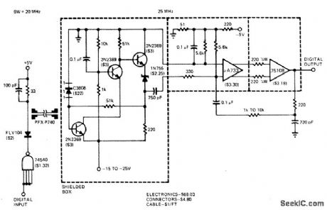
High data-rate capability for square-wave pulses is achieved by increasing complexity of receiver feeding digital output to microprocessor from remote teleprinter. Preamp design compensates for noise over limited frequency range, giving uniform S/ N ratio to about 20 MHz. With demonstration setup, visible-spectrum LED and photodetector shown performed acceptably with 40-foot cable.-O. E. Malvel and J. C. Freeborn, A Little Hands-On Experience llluminates Fiber-Optic Links, EDN Magazine, Nov. 5, 1977, p 71-75. (View)
View full Circuit Diagram | Comments | Reading(597)
EXPONENTIAL_DECAY_LOAD
Published:2009/7/24 2:45:00 Author:Jessie

Used in place of a capacitor when large load with expo nential decay is required. R1 provides means for monitoring current on cro. Article gives component values for wide range of decay limes, from 50 millisec to 1 sec, with initial discharge currents of 6.3 to 21.5 amp. Source voltage is 28 V.-B. Bever and L. Snyder, Transient Load With Exponential Decay, EEE, 10:10, p 31. (View)
View full Circuit Diagram | Comments | Reading(691)
50_MHz_40-W_amplifier_125_V_supply
Published:2009/7/24 2:44:00 Author:Jessie
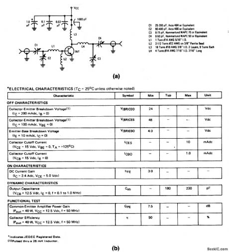
The electrical characteristics for the 2N5849 shown in this circuit are given in Fig.2-29B (View)
View full Circuit Diagram | Comments | Reading(747)
High_noise_rejection_thermometer
Published:2009/7/24 2:44:00 Author:Jessie

Pig. 13-26 This circuit makes it possible to transmit the temperature sensor output directly over an unshielded wire, with high noise immunity. Once calibrated with sensor and connecting wires in place, the circuit provides a typical ±2.0℃ accuracy-even in high-noise environments. To calibrate the thermometer, place the op-amp sensor in a +1℃ environment, and trim the 10℃ adjustment for an appropriate meter indication. Next, place the sensor in a +40℃ environment, and trim the 40℃ adjustment. Repeat the procedure until both points are fixed. Linear Technology Linear Applications Handbook 1990 p AN9-17. (View)
View full Circuit Diagram | Comments | Reading(673)
RADAR_RANGE_TESTER
Published:2009/7/24 2:44:00 Author:Jessie

Dynamic target simulator independently generates time-delayed fixed or moving target pulses for target rates above mach 3, for testing range accuracy of airborne automatic-tracking radar.-O. B. Mitchell, Simulator Tests Radar Trucking Systems, Electronics, 34:8, p 51-53. (View)
View full Circuit Diagram | Comments | Reading(791)
HIGH_SENSITIVITY_FIELD_STRENGTH_METER
Published:2009/7/2 2:07:00 Author:May

A TL081 (IC1 op amp is used to increase sensitivity. RF signal is detected by CR1 and is then amplified by IC1. Full-scale sensitivity is set with the 100 K potentiometer. (View)
View full Circuit Diagram | Comments | Reading(1188)
Double_ended_voltage_monitor
Published:2009/7/24 2:44:00 Author:Jessie


This circuit is similar to that of Fig. 8-26, except that the LED flash rate increases when the supply goes above 6 V, but below 15 V. The flash rate approaches zero near either limit. The minimum operating threshold is given by:
The maximum operating threshold is given by:
Typical circuit power drain is about 500 μA.
(View)
View full Circuit Diagram | Comments | Reading(1374)
Thermocouple_to_frequency_converter
Published:2009/7/24 2:43:00 Author:Jessie

Fig. 13-25 This circuit also provides temperature-to-frequency conversion, but it uses the popular type-K thermocouple as a sensor (instead of a temperature sensor as does the circuit of Fig. 13-24). To calibrate it, place the thermocouple in a 60℃ environment, and adjust the 50-kΩ potentiometer for 600 Hz output. Note that beyond 60℃, the cold-junction network departs from the thermocouple's response and causes output errors to increase rapidly. Linear technology Linear Applications Handbook 1990, p. AN7-3. (View)
View full Circuit Diagram | Comments | Reading(1534)
PINK_NOISE_GENERATOR
Published:2009/7/2 2:06:00 Author:May
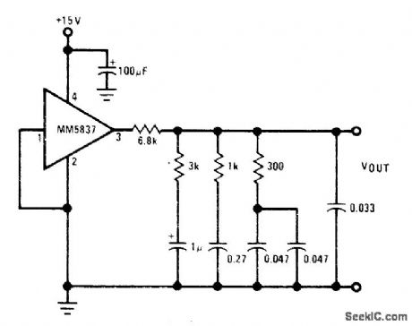
Uses MM5837 broadband white-noise generator with -3 dB per octave filter from 10 Hz to 40 kHz to give pink-noise output having flat spectral distribution over entire audio band from 20 Hz to 20 kHz.Output is about 1 V P-P of pink noise riding on 8.5-VOC level. Used as controlled source of noise for adjusting octave equalizer to optimum settings for specific listening area.- Audio Handbook. National Semiconductor. Santa Clara. CA. 1977. p 2-53-2-59. (View)
View full Circuit Diagram | Comments | Reading(4155)
| Pages:1157/2234 At 2011411142114311441145114611471148114911501151115211531154115511561157115811591160Under 20 |
Circuit Categories
power supply circuit
Amplifier Circuit
Basic Circuit
LED and Light Circuit
Sensor Circuit
Signal Processing
Electrical Equipment Circuit
Control Circuit
Remote Control Circuit
A/D-D/A Converter Circuit
Audio Circuit
Measuring and Test Circuit
Communication Circuit
Computer-Related Circuit
555 Circuit
Automotive Circuit
Repairing Circuit