
Circuit Diagram
Index 1143
3_1_TRACKING_FILTER
Published:2009/7/2 8:40:00 Author:May

Connection shown for Exar XR-215 PLL IC tracks input signal over 3:1 frequency range centered on free,running frequency of VCO. Tracking range is maximum when pin 10 is open. R0 is typically between 1K and 4K.C1 is between 30 and 300 times C0 where timing capacitor C0 depends on center frequency. System can also be operated as linear discriminator or analog frequency meter covering same 3:1 change of input frequency. RF can be 36K.- Phase-Locked Loop Data Book, Exar Integrated Systems, Sunnyvale, GA, 1978, p 21-28. (View)
View full Circuit Diagram | Comments | Reading(761)
STATE_VARIABLE_DESIGN
Published:2009/7/2 8:38:00 Author:May
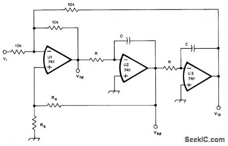
Universal filter network using three opamps can provide low-pass, high-pass, or bandpass audio response for CW and SSB reception. Filter uses one summing block U1, two identical integrators, U2 and U3, and one damping network. Cutoff frequencies are same as center frequency for bandpass response. Article gives design equations and graph for choosing values to give optimum performance for type of response desired, For unity-gain second-order Butterworth filter with low-pass or high-pass cutoff of 700 Hz, R is 6800 ohms and C is 0.033 μF. Q must be fixed at 0.707 and RA must equal 1.12 × RB. Thus, if RB is 2700 ohms, RA should be 3OOO.-H. M. Berlin, The State-Variable Filter, QST, April 1978, p 14-16. (View)
View full Circuit Diagram | Comments | Reading(695)
POSTAMPLIFIER_FOR_OPAMP
Published:2009/7/2 8:38:00 Author:May

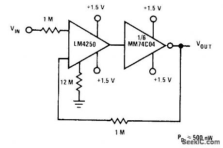
High input impedance of National MM74CO4 invertermakes it ideal for isolating load from output of LM425O micropower opamp operating from single dry cell- Linear Applications.vol.2. National Semiconductor. Santa Clara.CA. 1976,AN-88.p2 (View)
View full Circuit Diagram | Comments | Reading(455)
3_kHz_NOTCH
Published:2009/7/2 8:37:00 Author:May
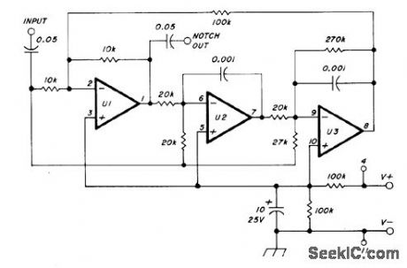
Uses three sections of National LM324 quad opamp to provide fixed center frequency of 3 kHz for notch. Single supply can be 5-25 V.-P. A. Lovelock, Discrete Operational Amplifier Active Filters, Ham Radio, Feb. 1978, p 70-73. (View)
View full Circuit Diagram | Comments | Reading(784)
TRACKING_QUAD_GAIN_CONTROL
Published:2009/7/2 8:31:00 Author:May
Basic circuit for each channel uses section of National LM324 quad opamp with section of AH5009 quad FET in feedback path. Each channel is AC coupled and has 40-dB range (gain range of 1 to 100).Bandwidth is minimum of 10 kHz. and S/N ratio is better than 70 dB with 4.3-VRMS maxi-mum output.-J. Sherwin, A Linear Multiple Gain-Controlled Amplifier. National Semiconductor. Santa Clara. CA. 1975. AN-129. p 6. (View)
View full Circuit Diagram | Comments | Reading(607)
OPTIMIZING_CMR
Published:2009/7/2 8:26:00 Author:May
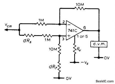
Article covers procedures for optimizing common-mode rejection when opamp is used to drive digital voltmeter. Value of Rv is determined by using resistance box connected between negative supply and pin 1 or 5 while other pin is shorted to negative supply, choosing pin which gives voltage swing in right direction on meter, then adiusting resistance box for zero output. Resistance box is similarly used at dR5 and dRf locations.-R. J. lsaacs, Optimizing OpAmps. Wireless World. April 1973. p 185-186. (View)
View full Circuit Diagram | Comments | Reading(511)
12_μH_GYRATOR
Published:2009/7/2 8:19:00 Author:May
Two RCA opamps in gyrator loaded with 10μ capacitor give effective 12-μH inductor that remains constant in value over rangefrom lOHz to almost 1 MHz.Q varies from 1 at l0Hz to maximum of 500 at 10 kHz,Article gives design equations.-A C Caggiano Simple Gyrator for L from C.EEE Magazine.Aug 1970.p 78. (View)
View full Circuit Diagram | Comments | Reading(751)
Bar_graph_temperature_display_dot_mode
Published:2009/7/24 2:13:00 Author:Jessie

Fig. 13-9 This circuit combines an LM34 temperature sensor, two LM3914 display drivers, and 20 LEDs to form a temperature display where the temperature is indicated by turn-on of the corresponding LED (from 67 to 86°F). The temperature range can be increased by cascading several LM3419s. The display can be converted from the dot mode to the bar mode, or to flash a bar of LEDs when the temperature sensed reaches a selected limit. This requires a few extra components, as shown on the LM3419 datasheet. Note that the trim values for VA, VB and 1/C are for the temperature range show. UB and VC represent the highest and lowest temperatures, respectively. VA is set for gain of 4 (40 mV/°F instead of the nominal 10 mV/'F provided by the LM34). National Semiconductor Linear Applications Handbook 1991 p 1077. (View)
View full Circuit Diagram | Comments | Reading(5482)
2_20_kHz_SELF_TUNING_BANDPASS
Published:2009/7/2 8:13:00 Author:May

Center frequency of filter is automatically adjusted to track signal frequency, for optimum noise rejection when input frequency varies over wide range as it does with many types of vibrating transducers.Requires no reference frequency and no intemal oscillator or synchronizing circuits. Flequency range can be extended in decade steps by capacitor switching. When filter is not tuned to input frequency, phase shift is not 180° and phase detector applies error signal to gate of FET to control its drain-source resistance. Phase detector A4-A5-CR2-CR3 and FET form part of negative-feedback loop around filter, so error in phase changes resistance of FET and thereby retunes filter, Article gives design equations, operational details, and waveforms at various points in circuit.-G. J. Deboo and R.C. Hedlund, Automatically Tuned Filter Uses IC Operational Amplifiers, EDN/EEE Magazine, Feb.1, 1972, p 38-41. (View)
View full Circuit Diagram | Comments | Reading(913)
75O_Hz_SIXTH_ORDER_BANDPASS
Published:2009/7/2 8:12:00 Author:May

Provides passband gain of 6 (15.6 dB) and Q of 8.53 by cascading three identical second-order filter sections. Each section uses multiple feedback.-H. M.Berlin, Design of Active Filters, with Experiments, Howard W. Sams, Indianapolis, IN, 1977, p 147-148. (View)
View full Circuit Diagram | Comments | Reading(808)
HEAT_PROGRAM_TIMER
Published:2009/7/24 2:12:00 Author:Jessie

Controls weld energy for production-line welding of electron tubes and other small components. Functions controlled are low heat, weld heat, up-slope time, weld time, and down-slope time. Adjustable potentiometers permit changing each of these times.-A. V. Ronis, Heat Program Timer Controls Weld Energy, Electronics, 31:23, p 76-78. (View)
View full Circuit Diagram | Comments | Reading(659)
150_Hz_HIGH_PASS
Published:2009/7/2 8:10:00 Author:May

Circuit includes variable high-frequency source supplying triangle-wave input to filter for demonstrating high-pass action. If long supply leads cause oscillation, connect 0.1-μF capacitors between ground and supply pins 4 and 7 as shown.-F. M. Mims, lntegrated Circuit Projects, Vol. 4, Radio Shack, Fort Worth, TX, 1977, 2nd Ed., p 87-94. (View)
View full Circuit Diagram | Comments | Reading(934)
LOW_COST_FET_INPUT
Published:2009/7/2 8:09:00 Author:May

Uses two 2N3819 FETs as differential source-follower operated at constant source current of 200μ A provided by Tr1.and Tr2. Input performance is comparable to that of more expensive commercial units. Match FETs to reduce thermal drift. Trim input offset voltage to zero by adding resistor in appropriate FET source. Input impedance of circuit is greater than 1013 ohms.-J. Setton. F.E.T.-Input Operational Amplifier. Wireless World. Nov. 1976. p 61. (View)
View full Circuit Diagram | Comments | Reading(695)
SQUARE_WAVES_FROM_MVBR
Published:2009/7/24 2:12:00 Author:Jessie
Use of four additional components (two resistors and two diodes) with basic free-running mvbr changes its output to dean square wave. Operating range is from several cps to several Mc.-R. O. Gregory and J. C. Bowers, Simple Square-Wave Generator, Electronics, 35:51, p 47. (View)
View full Circuit Diagram | Comments | Reading(609)
18_dB_PER_OCTAVE_EMPHASIS
Published:2009/7/2 8:09:00 Author:May
Circuit shown is result of design procedure given in article for active filter that provides frequency emphasis at rate of 18 dB per octave between 5 and 15 kHz, Emphasis does not exceed 40 dB at 20 kHz.Design equations include parameters for closed-loop gain of opamp. Scale factor is applied to input and feedback networks individually after design, to give reasonable eomponent values.-B. Brandstedt, Tailor the Response of Your Active Filters, EDN magazine, March 5, 1973, p 68-72. (View)
View full Circuit Diagram | Comments | Reading(560)
FM_IF_PLI_detector_double_conversion_and_RF_mixer
Published:2009/7/24 2:12:00 Author:Jessie
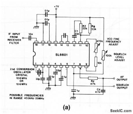
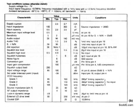
The SL6601 used in this circuit is a straight-through or single-conversion IF amplifier and detector for FM-radio applications. Figure 2-10B shows the electrical characteristics. A typical value for timing capacitor C is 390 pF. (View)
View full Circuit Diagram | Comments | Reading(1205)
300_3000_Hz_WIDEBAND
Published:2009/7/2 8:07:00 Author:May

Used in voice communication systems where signals below 300 Hz and above 3000 Hz must be rejected. Secondorder Butterworth stopband responses are achieved by combining low-pass and high-pass sections of equal-component voltage-controlled voltage-source filters. Overall passband gain is 8 dB Opamps can be 741.-H. M. Berlin, Design of Active Filters, with Experiments, Howard W. Sams, Indianapolis, IN, 1977, p 148-151. (View)
View full Circuit Diagram | Comments | Reading(1320)
480_kHz_LOW_PASS
Published:2009/7/2 8:07:00 Author:May

Butterworth low-pass active filter uses pair of dual opamps with external resistors and capacitors to give corner frquency of 480 kHz and output impedance level of 1K. Article presents design procedure in detail and gives frequency response curve.-L. T.Burton and D.Treleaven, Active Filter Design Using Generalized Impedance Conveners, EDN Magazine,Feb.5,1973, p 68-75. (View)
View full Circuit Diagram | Comments | Reading(796)
BUFFERED_OPAMP
Published:2009/7/2 8:03:00 Author:May
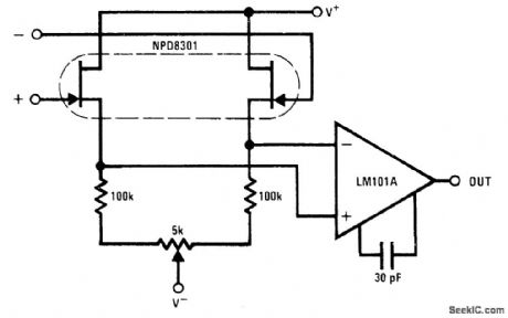
NPD8301 dual FET is ideal low-offset low-drift buffer for LM101A opamp. Matched sections of FET track well over entire bias range, for improved common-mode re jec-ion.- FET Databook. National Semiconductor. Santa Clara. CA. 1977. p 6-26-6-36. (View)
View full Circuit Diagram | Comments | Reading(832)
13O_V_P_P_DRIV
Published:2009/7/2 8:00:00 Author:May
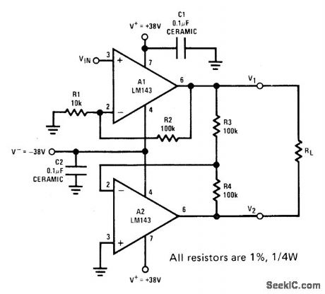
Two LM143 high-voltage opamps operating from 38-V supply can provide up to 138 V P-P undipped into 10K floating Ioad when connected as shown to give noninverting voltage amplifier followed by unity-gaininverter. Power supplies should be bypassed to ground with 0.1-μF capacitors. - Linear Applications, Vol. 2. National Semiconductor, Santa Clara. CA. 1976. AN-127. p 1-3. (View)
View full Circuit Diagram | Comments | Reading(555)
| Pages:1143/2234 At 2011411142114311441145114611471148114911501151115211531154115511561157115811591160Under 20 |
Circuit Categories
power supply circuit
Amplifier Circuit
Basic Circuit
LED and Light Circuit
Sensor Circuit
Signal Processing
Electrical Equipment Circuit
Control Circuit
Remote Control Circuit
A/D-D/A Converter Circuit
Audio Circuit
Measuring and Test Circuit
Communication Circuit
Computer-Related Circuit
555 Circuit
Automotive Circuit
Repairing Circuit