
Circuit Diagram
Index 1151
DIFFERENTIAL_INPUT_A_D_SYSTEM
Published:2009/7/2 4:06:00 Author:May

Using a CA3140 BiMOS op amp provides good slewing capability for high bandwidth input signals, and can quickly settle energy that the CA3310 outputs at its VIN terminal. The CA3140 can also drive close to the negative supply rail. If system supply sequencing or an unknown input voltage is likely to cause the op amp to drive above the VDD supply, a diode clamp can be added from pin 8 of the op amp to the VDD supply. (View)
View full Circuit Diagram | Comments | Reading(1015)
AUTOMATIC_STEREO_SWITCH
Published:2009/7/24 3:08:00 Author:Jessie
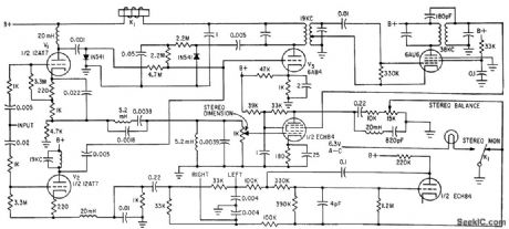
Switches f-m tuner info stereo mode and turns on indicator lamp when f-m tuner is tuned to station broadcasting stereo subcarrier or when subcarrier comes on during normal f-m broad.cast.-L. Solomon, Audio Show Features Automatic Stereo, Hi-Fi Earphones, Electronics, 34:39, p 34-35. (View)
View full Circuit Diagram | Comments | Reading(690)
CYCLIC_A_D_CONVERTER
Published:2009/7/2 4:04:00 Author:May

The cydic converter consists of a chain of identical stages, each of which senses the polarity of the input. The stage then subtracts VREF from the input and doubles the remainder if the polarity was correct. The signal is full-wave rectifted and the remainder of VIN - VREF is doubled. A chain of these stages gives the gray code equivalent of the input voltage in digitized form related to the magnitude of VREF. Possessing high potential accuracy, the circuit using NE531 devices settles in 5 μs. (View)
View full Circuit Diagram | Comments | Reading(909)
Centigrade_thermometer_with_cold_junction_compensation
Published:2009/7/24 3:08:00 Author:Jessie


Fig. 13-40 This circuit is an electronic thermometer with a 10 mV/℃ output from 0℃ to 1300℃. To trim, first short out the LM329B, the LM335 and the thermocouple. Measure and record the output voltage from A1 (this should be equal to the input offset voltage of A1 times the voltage gain). Remove the short from the thermocouple and apply a 50-mV input to A1 and adjust the 5-kΩ gain potentiometer until the A1 output voltage is 12.25 V above the previously recorded value. Short out the thermocouple again, but remove the short across the LM335. Adjust the 10-kΩ TC potentiometer so that the output voltage from A1 equals 10 mV/°K times the absolute temperature. Finally, remove the short across the LM329B and adjust the 10-kΩ zero potentiometer so that the A1 output voltage equals 10 mV/℃ times the ambient temperature in 0℃. The table of Fig. 13-40B shows the error resulting from thermocouple nonlinearity as a function of temperature. National Semiconductor Linear Applications Handbook 1991, p. 524, 525. (View)
View full Circuit Diagram | Comments | Reading(2958)
X100_instrumentation_amplifier
Published:2009/7/24 3:08:00 Author:Jessie

This circuit requires two 1.5-V cells connected directly (no power switch) to the V+ and V- terminals. Total current drain is 2.8 μA. R11 matches gains of Al and A2 to get maximum common-mode rejection ratio. Figure 8-32B shows both CMRR and voltage gain across frequency range. C1 balances wiring (rather than amplifier frequency response) to give an additional 10 to 20 dB of CMRR. Maximum peak-to-peak output into a 100-kΩ load is about 1.8 V. When doing power measurements on this circuit, remember that even a 1-MΩ scope probe placed between +1.5 V and -1.5 V more than doubles the power drawn from the batteries. (View)
View full Circuit Diagram | Comments | Reading(710)
225_to_400_MHz_60_W_broadband_amplifier_28_V_supply
Published:2009/7/24 3:07:00 Author:Jessie

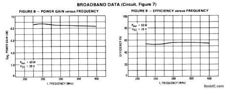
The electrical characteristics for the 2N6439 shown in this circuit are given in Fig.2-39B. (View)
View full Circuit Diagram | Comments | Reading(626)
Temperature_controller_for_quartz_crystal_ovens
Published:2009/7/24 2:59:00 Author:Jessie

Fig. 13-35 This circuit will provide temperature control for an oven at 75℃, which is ideal for most types of quartz crystals. The temperature setpoint is established by the LM103-3.9 reference and the 1- to 6.8-kΩ divider. In practice, the LM335 should be in good thermal contact with the heater to prevent servo oscillation. National Semiconductor. Linear Applications Handbook 1991 p 839. (View)
View full Circuit Diagram | Comments | Reading(1481)
SEQUENCE_DETECTOR
Published:2009/7/2 4:04:00 Author:May


Generates output pulse if, and only if, sequence of input pulses is in prescribed order. Any other sequence inhibits output pulse and clears circuit at instant of first out-of-order pulse. Circuit also clears itself at end of correct sequence, by generating sequence-OK pulse. Developed for use in control systems, electronic combination locks, and any other applications requiring sequence of pulses.To detect more than 4 bits in sequence, NAND gates and flip-flops can be added. If TTL input pulses occur in correct T1-T2-T3-T4 order, 1 state at U1D1 will propagate down chain of D flip-flops until U2Q2 output is reached. Simultaneously, 0 is propagated in similar manner to hold dear bus at 1. Article traces circuit operation in detaiL-M. J. Gallagher, Seff-Clearing Digital Sequence Detector, EDN Magazine, April 5, 1973, p88-89. (View)
View full Circuit Diagram | Comments | Reading(1600)
10_MINUTE_STEPPED_SWEEP
Published:2009/7/24 2:59:00 Author:Jessie

Provides long stepped sweeps required for swept-frequency ionosondes, with 100-v amplitude. Schmitt trigger V3 detects end of rundown and initiates recharging of C1.-K. Perry, Long Staircase Generator, Electronics, 35:35, p 54. (View)
View full Circuit Diagram | Comments | Reading(621)
SUCCESSIVE_APPROXIMATION_A_D_CONVERTER_1
Published:2009/7/2 4:02:00 Author:May

The 10-bit conversion time is 3.3 μs with a 3 MHz clock. This converter uses a 2504 12-bit successive approximation register in the short cycle operating mode where the end of conversion signal is taken from the first unused bit of the SAR (Q10). (View)
View full Circuit Diagram | Comments | Reading(1007)
200_MHz_narrowband_amplifier_15_V_supply
Published:2009/7/24 2:49:00 Author:Jessie
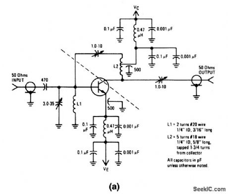
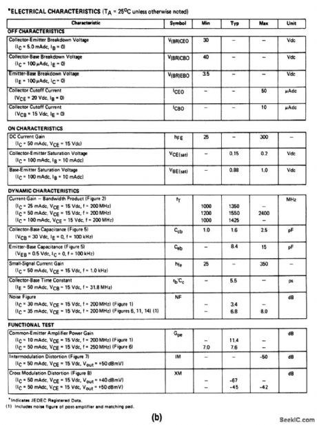
The electrical characteristics for the 2N5943 shown in this circuit are given in Fig. 2-31B. (View)
View full Circuit Diagram | Comments | Reading(735)
POWER_SUPPLY_FOR_25_WATT_ARC_LAMP
Published:2009/7/2 4:01:00 Author:May
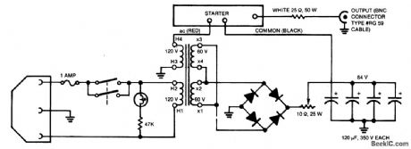
Circuit NotesA dual-voltage circuitry both strikes and maintains the arc.The lamps require a starting voltage in excess of 1,000 volts. Once stabilized, the voltage drop across the lamp is near 20 volts. Power supply consists of two main sections. The first section, the low-voltage power supply section, is an 84-volt direct-current supply.This supply powers the stabilized arc. Current is limited by the 10 ohm adjustable and 25 ohm fixed resis-tance. The second section, the high-voltage starter circuit, is a Cockroft-Walton voltage multiplier. With no load, the output voltage is 2,036 volts. However, when the arc is established, the heavy current drain maintains a forward bias on all of the diodes, and the circuit becomes a straight path with a voltage drop of 7.2 volts. The small value of the capacitors used in the multiplier guarantees that the diodes will be forward-biased once the arc is established. (View)
View full Circuit Diagram | Comments | Reading(1324)
High_efficiency_inverter_with_adjustable_output
Published:2009/7/24 2:48:00 Author:Jessie


Figure 7-66 shows the MAX764/65/66 connected to provide inverter operation with an adjustable output (-1.0 V to -16 V). For adjustable operation, let R1= 150 kΩ, then find the value of R2 using: Where VREF = 1.5 V. See Fig. 7-65 for component suppliers. MAXIM NEW RELEASES DATA Book, 1995, P. 4-121. (View)
View full Circuit Diagram | Comments | Reading(828)
HIGH_SPEED_12_BIT_A_D_CONVERTER
Published:2009/7/2 4:00:00 Author:May

This system completes a full 12-bit conversion in 10 μs unipolar or bipolar. This converter will 6e accurate to ±1/2 LSB of 12 bits and have a typical gain TC of 10 ppm/℃. In the unipolar mode, the system range is 0 V to 9.9976 V, with each bit having a value of 2.44 mV. For the true conversion accuracy, an A/D converter should be trimmed so that given bit code output results from input levels from 1/2 LSB below to 1/2 LSB above the exact voltage which that code represents. Therefore, the converter zero point should be trimmed with an input voltage of 1.22 mV; trim R1 until the LSB just begins to appear in the output code (all other bits 0 ). For full-scale, use an input voltage of 9.9963 V (10 V-1 LSB-1/2 LSB); then trim R2 until the LSB just begins to appear (all other bits 1 ). The bipolar signal range is -5.0 V to 4.9976 V. Bipolar offset trimming is done by applying a -4.9988 V input signal and trimming R3 for the LSB transition (all other bits 0 ). Full-scale is set by applying 4.9963 V and trimming R2 for the LSB transition (all other bits 1 ). (View)
View full Circuit Diagram | Comments | Reading(1144)
PHASE_SENSITIVE_DETECTOR
Published:2009/7/2 3:57:00 Author:May

Uses quadruple two-input NAND-gate IC with minimum of external components. DC output level is absolutely linear with phase difference at inputs, making circuit suitable for phase-locked loops and phase-shift keyed demodulation. Output is rectangular wave whose mark-space ratio is proportional to phase difference between input square waves. This output is applied to lowpass filter R2-C1, having values chosen to suit operating frequency and required output resistance. R1 is chosen to give required output swing up to maximum of 15 V.-R. A. Harrold, Inexpensive P.S.D., Wireless World, Jan. 1973, p32. (View)
View full Circuit Diagram | Comments | Reading(2481)
Thermistor_signal_conditioner_for_current_loops
Published:2009/7/24 2:48:00 Author:Jessie

Fig. 13-28 This circuit shows a complete 2-wire thermistor temperature-transducer interface with a 4- to 20-mA output. The 4- to 20-mA current-loop control is common in industrial environments. The circuits used to modulate transducer data in a 4- to 20-mA loop must operate well below the 4-mA minimum current. Over a 0 to 100℃ range, accuracy is ±0.3℃ and the circuit is current-loop powered (no external supply is required). Trims shown are for 0℃ and 100℃, and are made by exposing the thermistors to those temperatures. The thermistor datasheets show methods for electrically simulating 0℃ and 100℃, Linear Technology Linear Applications Handbook, 1990 p AN23-5 . (View)
View full Circuit Diagram | Comments | Reading(1281)
10-BIT_A_D_CONVERTER
Published:2009/7/2 3:56:00 Author:May


The converter has a 60 ms conversion time, consumes 460 μA from its 1.5 V supply and maintains 10 bit accuracy over a 15℃ to 35℃ temperature range. A pulse applied to the convert command line causes Q3, operating in inverted mode, to discharge through the 10 kΩ diode path, forcing its collector low. Q3's inverted mode switching results in a capacitor discharge within 1 mV of ground. During the time the ramps' value is below the input voltage, CIA's output is low. This allows pulses from C1B, a quartz stabilized oscillator, to modulate Q4. Output data appears at Q4's collector. When the ramp crosses the input voltages value C1A's output goes high, biasing Q4 and output data ceases. The number of pulses at the output is directly proportional to the input voltage. To calibrate apply 0.5 V to the input and trim the 10 kΩ potentiometer for exactly 1000 pulses out each time the convert command line is pulsed. (View)
View full Circuit Diagram | Comments | Reading(1079)
BIPOLAR_POWER_SUPPLY_FOR_BATTERY_INSTRUMENTS
Published:2009/7/2 3:54:00 Author:May

Circuit NotesTo generate regulated ±5-V supplies from a pair of dry batteries, the circuit of Fig.1 is commonly used. In order to give protection from inadvertent reverse connection of a battery, a diode in series with each battery would produce an unacceptable voltage drop. The more effective approach is to fit diodes D1 and D2 as shown in Fig. 2, in parallel with each battery.When the supply is switched off, there is the risk of a reverse bias being applied across the regulators, if there is significant inductance or capacitance in the load circuit.Diodes across the regulators prevent damage. When the power supply is switched on, the two switches do not act in unison. There is a probability that one or the other regulators will be latched hard off by the other. To prevent this, D3 and D4 are Zener diodes so that ±5-V rails are pulled up by the batteries until the regulators establish the correct levels. (View)
View full Circuit Diagram | Comments | Reading(956)
IONOSPHERIC_SOUNDER_PULSE_SIMULATOR
Published:2009/7/24 2:47:00 Author:Jessie

Generates long and short output pulses with positive and negative polarities, each adjustable in duration and amplitude. Small pulse can be moved through large pulse. Simulator is triggered at power-line frequency.-K. Perry, Back-Scatter Simulator Checks lonospheric Sounder Displays, Electronics, 35:25, p 50. (View)
View full Circuit Diagram | Comments | Reading(546)
AND_LOGIC_FOR_MUTlNG
Published:2009/7/2 3:53:00 Author:May
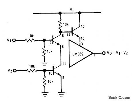
Connection shown for National LM389 combination of three transistors with opamp gives standard AND circuit for controlling muting transistor in audio sys tem. Shorting pin 12 of opamp to ground gives NAND Iogic.- Audio Handbook, National Semiconductor, Santa Clara, CA, 1977, p 4-33-4-37. (View)
View full Circuit Diagram | Comments | Reading(602)
| Pages:1151/2234 At 2011411142114311441145114611471148114911501151115211531154115511561157115811591160Under 20 |
Circuit Categories
power supply circuit
Amplifier Circuit
Basic Circuit
LED and Light Circuit
Sensor Circuit
Signal Processing
Electrical Equipment Circuit
Control Circuit
Remote Control Circuit
A/D-D/A Converter Circuit
Audio Circuit
Measuring and Test Circuit
Communication Circuit
Computer-Related Circuit
555 Circuit
Automotive Circuit
Repairing Circuit