
Circuit Diagram
Index 1146
DC_TO_DC_SMPS_VARIABLE_18_V_TO_30_V_OUT_AT_02_A
Published:2009/7/2 5:29:00 Author:May

View full Circuit Diagram | Comments | Reading(581)
PULSE_WIDTH_DETECTOR
Published:2009/7/2 5:27:00 Author:May

Logic terminal of National LM122 timer is driven simultaneously with trigger input to give high-accuracy pulsewidth detector. Output changes state onlv when trigger input stays high for longer than time period set by Rt and Ct; resulting output pulse width is then equal to input trigger width minus RtCt. CL filters out narrow spikes that would occur at output due to interval delays during switching. Supply can range from 4.5 to 4O V.-C. Nelson, Versatile Timer Operates from Microseconds to Hours, National Semi-conductor, Santa Clara, CA, 1973, AN-97, p 9. (View)
View full Circuit Diagram | Comments | Reading(2840)
TIMING_SIGNAL_GENERATOR
Published:2009/7/24 2:16:00 Author:Jessie

Delivers pulses of controlled duration, amplitude, and carrier content at 1 pps in channel A and either 1 per 5 sec or 1 per 10 sec in channel B. Any decimal frequency multiple of 1, 2, or 5 from 100 to 0.1 cps may be obtained. Timed pulse signals can be controlled both in amplitude and width, and turned on or off at will.-D. E. Minow, Timed-Singal Generator With Flexible Output, Electronics, 32:10, p 52-53. (View)
View full Circuit Diagram | Comments | Reading(612)
12_14_V_REGULATED_3_A_POWER_SUPPLY
Published:2009/7/2 5:27:00 Author:May

View full Circuit Diagram | Comments | Reading(624)
LOW_LEVEL_ACTIVATION_BY_CMOS
Published:2009/7/2 5:23:00 Author:May

Typical CMOS gate interf aces directly with small-signal Darlington transistor driving 80-mA lamp load.-A. Pshaenich, Interface Techniques Between industrial Logie and Power Devices, Motorola, Phoenix, AZ, 1975, AN-712A, p 11. (View)
View full Circuit Diagram | Comments | Reading(605)
175_MHz_25_W_amplifier_28_V_supply
Published:2009/7/24 2:16:00 Author:Jessie

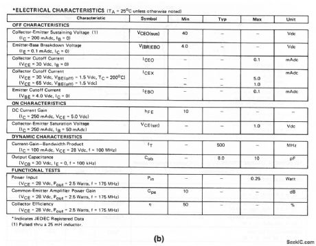
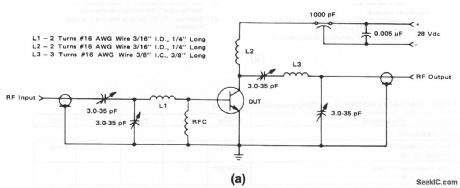


The electrical characteristics for the 2N3553 shown in this circuit are given in Fig. 2-12B. (View)
View full Circuit Diagram | Comments | Reading(1378)
90_V_rms_VOLTAGE_REGULATOR_USING_A_PUT
Published:2009/7/2 5:23:00 Author:May

Circuit Notes
The circuit is an open loop rms voltage regulator that will provide 500 watts of power at 90 V rms with good regulation for an input voltage range of 110-130 V rms. With the input voltage applied, capacitor C1 charges until the firing point of Q3 is reached causing it to fire. This turns Q5 on which allows current to flow through the load. As the input voltage increases, the voltage across RIO increases which increases the firing point of Q3. This delays the firing of Q3 because C1 now has to charge to a higher volt-age before the peak-point voltage is reached. Thus the output voltage is held fairly con-stant by delaying the firing of Q5 as the input voltage increases. For a decrease in the input voltage, the reverse occurs. (View)
View full Circuit Diagram | Comments | Reading(891)
Proportional_temperature_controller
Published:2009/7/24 2:16:00 Author:Jessie

Fig. 13-11 Here, an LM10 serves as both a temperature-setting device and as a driver for the heating unit (an LM395 power transistor). The optional lamp, driven by an LP395, indicates if power is applied to the heater. When a change in temperature is desired, the user adjusts the 50-kΩ pot and the circuit makes the temperature transition with a minimum of overshoot or ringing. The circuit is calibrated by selection of R2, R3, and C2 for minimum overshoot. C2 eliminates dc offset errors. R1 and C1 are added to improve loop stability about the temperature-set point. For optimum performance, locate the temperature sensor LM34 as close as possible to the heater. This will minimize time lag between the heater and sensing. Long-term stability and repeatability are better than 0.5°F. National Semiconductor Linear Applications Handbook, 1991. p 1079 (View)
View full Circuit Diagram | Comments | Reading(0)
SCHMITT_USING_7400_GATES
Published:2009/7/2 5:20:00 Author:May
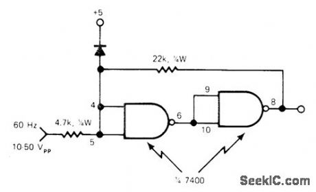
Uses two sections of 7400 quad NAND gate. Will accept input voltages of 10-50 V P-P with values shown, but can use line voltage directly if input resistor is 22K and feedback resistor is 220K. Diode in DC supply limits positive-going input to 5.7 V forprotection of input circuit. Used as interface between 60-Hz line and frequency divider having TTL logic, when 1-s time base is required for timing applications.-W. A. Palm, Connect a 7400 Gate as a Schmitt Trigger, EDN Magazine, Aug. 20, 1976, p 84. (View)
View full Circuit Diagram | Comments | Reading(742)
OR_LOGIC_FOR_MUTlNG
Published:2009/7/2 5:17:00 Author:May
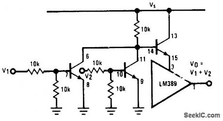
Connection shown for National LM389 combination of three transistots with opamp gives standard OR circuitfor controlling muting transistor in audio system.Shorting pin 12 of opamp to ground gives NOR logic.- Audio Handbook, National Semiconductor, Santa Clara, CA, 1977, p 4-33-4-37. (View)
View full Circuit Diagram | Comments | Reading(540)
FOUR_FUNCTION__WELDING_TIMER
Published:2009/7/24 2:15:00 Author:Jessie

Thyratrons serve as relays for controlling squeeze time, weld time, hold time, and off time in high-speed resistance welding, Control Provides fail-safe operation, reduces transients by accurraely adjusting ignitron firing angle, and gives accurate repetition of timing cycle.-S. C. Rocka fellow, Electronic Control Times High-Speed Welding cycle,Electronics,31:33,p 70-73. (View)
View full Circuit Diagram | Comments | Reading(1236)
ACTIVE_CW_FILTER
Published:2009/7/2 5:17:00 Author:May

Modifications made on MFJ Enterprises OWE-2 active audio filter per mit maximum flexibility. Circuit provides fixed bandwidth of 180 or 110 Hz centered on 750 Hz, or optional variable bandwidth for which center frequency can be adiusted in range of 280 to 1590 Hz.-H. M. Berlin, Increased Flexibility for the MFJ Enterprises CW Filters, Ham Radio, Dec. 1976, p 58-60. (View)
View full Circuit Diagram | Comments | Reading(1880)
PWN_MOTOR_SPEED_CONTROL
Published:2009/7/2 5:15:00 Author:May

Speed control is accomplished by pulse width modulating the gates of two MGP20N45 TMOS devices. Therefore, motor speed is proportional to the pulse width of the incoming digital signal, which can be generated by a microprocessor or digital logic.The incoming signal is applied to comparator U1, then to paralleled inverters U2, U3, and U4 that drive the two TMOS devices, which, in turn, control power applied to the motor armature. Bridge rectifier Dl supplies fullwave power that is filtered by R5 and C1. Free-wheeling diode D3 (MR854) prevents high voltage across Q1 and Q2.A back-to-back zener diode, D2, protects against transients and high voltage surges. (View)
View full Circuit Diagram | Comments | Reading(711)
Dual_transceiver_18_V_to_425_V
Published:2009/7/24 2:15:00 Author:Jessie


Figure 3-35 shows a typical application circuit for single-supply operation of the MAX218. Figure 3-36 shows the connections for operation from unregulated and regulated supplies. Figure 3-37 shows the pin descriptions. Figure 3-38 shows suggested component suppliers. This IC runs on two alkaline (NiCd or NiMH) cells to provide full EIA/TIA-232E and V.28/V.24 communications interface. True RS-232 and EIA/TIA-562 voltage levels are maintained with a wide +1.8-V to +4.25-V operating range. A shutdown mode reduces current to 1μA. The receivers can be enabled or disabled under logic control. Figure 3-39 shows the shutdown and enable/disable mode logic. The data rate is guaranteed at 120 kbps. MAXIM NEW RELEASES DATA BOOK, 1995, P. 2-79, 2-80, 2-81, 2-82. (View)
View full Circuit Diagram | Comments | Reading(608)
MOS_TO_TTL_DRIVER
Published:2009/7/2 5:14:00 Author:May
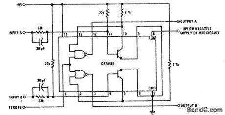
National DS75450 dual peripheral driver serves as interface between different logic types while providing highspeed switching and 300-mA output current per section Requires only single 5-V supply- Interface Databook, National Semiconductor、Santa Clara,CA,1978,p3-20-3-30 (View)
View full Circuit Diagram | Comments | Reading(542)
10_kHz_VOLTAGE_TUNED_
Published:2009/7/2 5:14:00 Author:May
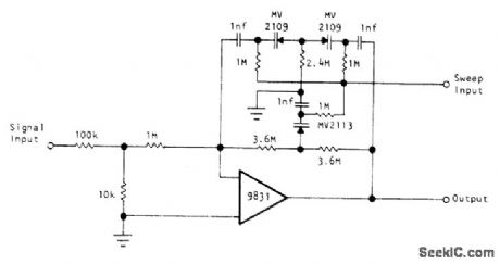
High-Q circuit using Optical Electronies 9831 opamp has sharp resonance, as required for analysis of spectrum of incoming signal. Reverse-biased silicon junctions senre as voltage variable capacitors for sweeping center frequency over 3: 1 range. Values shown for three resistors in twin-T network give cenW frequency of 10 kHz.- Voltage Tuned High-Q Filter, Optical Electronics, Tucson, AZ, Application Tip 10207. (View)
View full Circuit Diagram | Comments | Reading(599)
10_Hz_HIGH_PASS
Published:2009/7/2 5:13:00 Author:May

Equiterminated Butter-worth high-pass ladder filter has corner frequency of 10 Hz and output impedance level of 16K. Opamps are matched pair in single ML747 package. Article covers design procedure based on use of generalized impedance converters and gives frequency response curve.-L. T. Burton and D. Treleaven, Active Filter Design Using Generalized Impedance Converters, EDN Magazine,Feb. 5,1973,p 68-75. (View)
View full Circuit Diagram | Comments | Reading(1015)
METAL_FOIL_SPOTWELDING_CONTROL
Published:2009/7/24 2:15:00 Author:Jessie

Permits precise control of high-energy capacitor discharge used in welding extremely thin and highly conductive foils or fine wires. Heat control provides range of 650 to 1,500 v for level at which energy is stored, and selector switch gives choice of 50, 100, and 200 mfd for storage capacitor.-J. Markus, Handbook of Electronic Control Circuits, McGraw-Hill, New York, 1959, p 321. (View)
View full Circuit Diagram | Comments | Reading(1270)
THREE_LOUDSPEAKER_CROSSOVERS
Published:2009/7/2 5:12:00 Author:May

Active filter network splits AF input into three frequency bands each feeding separate 30-W power amplifier. Design allows adjustment of any part of frequency characteristic to any desired level and gives choice of slopes in any part of frequency band. Article gives design equa-tions and construction details. PNP transistors can be BCY70, BCY71, BCY72, or 2N3906. Article also gives circuit of suitable 30-W amplifier.-D. C.Read, Active Filter Crossover Networks, Wireless World, Dec.1973, p 574-576. (View)
View full Circuit Diagram | Comments | Reading(856)
SCHMITT_FROM_555_TIMER
Published:2009/7/2 5:11:00 Author:May

Only three additional parts need be added to standard 555 timer to give fully TTL/DTL-compatible Schmitt trigger that responds to slow input ramps as well as straight DC levels. With output initially high, increasing input from 0 to about 1.35V drives output low. Conversely, input can decrease to about 0.7 V before output goes high again.-M. K. Lalitha and P, R, Chetty, Variable-Threshold Sch mitt Tdgger Uses 555 Timer, EDN Magazine, Sept. 20, 1976, p 112 and 114. (View)
View full Circuit Diagram | Comments | Reading(993)
| Pages:1146/2234 At 2011411142114311441145114611471148114911501151115211531154115511561157115811591160Under 20 |
Circuit Categories
power supply circuit
Amplifier Circuit
Basic Circuit
LED and Light Circuit
Sensor Circuit
Signal Processing
Electrical Equipment Circuit
Control Circuit
Remote Control Circuit
A/D-D/A Converter Circuit
Audio Circuit
Measuring and Test Circuit
Communication Circuit
Computer-Related Circuit
555 Circuit
Automotive Circuit
Repairing Circuit