
Circuit Diagram
Index 1152
INEXPENSIVE,FAST_10_BIT_SERIAL_OUTPUT_A_D
Published:2009/7/2 3:53:00 Author:May

Everytime a pulse is applied to the convert command input, Q1 resets the 1000 pF capacitor to.0 V. This resetting action takes 200 ns of the falling edge of the convert command pulse, the capacitor begins to charge linearly. In precisely 10 microseconds, it charges to 2.5 V. The 10 microseconds ramp is applied to the LT1016's positive input. The LT1016 compares the ramp to Ex, the unknown, at its negative input. For a 0 V - 2.5 V range, Ex is applied to the 2.5 k ohm resistor. From a 0 V - 10 V range, the 2.5 k ohm resistor is grounded and Ex is applied to the 7.5 k ohm resistor. Output of the LT1016 is a pulse whose width is directly dependent on the value of Ex. This pulse width is used to gate a 100 MHz clock. The 100 MHz clock pulse bursts that appear at the output are proportional to Ex. For a 0 V - 10 V input, 1024 pulses appear at fullscale, 512 at 5.00 V, etc. (View)
View full Circuit Diagram | Comments | Reading(817)
LATCH
Published:2009/7/2 3:51:00 Author:May
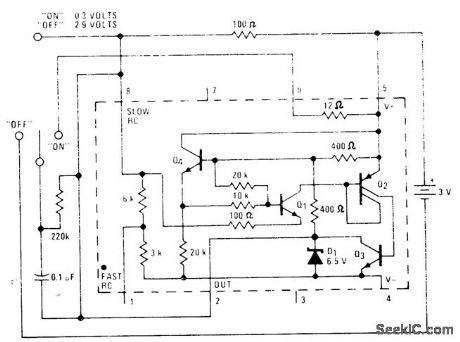
National LM3909 IC operating from 3-V battery requires only momentary contact by switch to change logic level of output and hold that level.- Linear Applications.Vol, 2, National Semiconductor, Santa Clara,CA,1976,AN-154,p9 (View)
View full Circuit Diagram | Comments | Reading(605)
16_BIT_A_D_CONVERTER
Published:2009/7/2 3:50:00 Author:May

The A/D converter, made up of A2, a flip-flop, some gates and a current sink, is based on a current balancing technique. Once again, the chopper-stabilized LTC1052's 50 nV/℃ input drift is required to eliminate offset errors in the A/D. (View)
View full Circuit Diagram | Comments | Reading(1048)
10_AMP_REGULATOR_WITH_CURRENT_AND_THERMAL_PROTECTION
Published:2009/7/2 3:50:00 Author:May

View full Circuit Diagram | Comments | Reading(1196)
NOISE_BLANKER
Published:2009/7/2 3:48:00 Author:May

Minimizes effects of shortduration high-amplitude low-repetition-rate noise such as auto ignition noise, power-line arcing, and make-or-break switching. Developed for use in Collins ARR-41 receiver, where it is inserted between plate of second mixer and 500-kHz first IF amplifier. Q1 and its doubletuned drain circuit form low-gain bandpass amplifier that removes remaining local oscillator signal and sets bandwidth at about 50 kHz. Signal is then split into two channels. Q2 in main channel drives 50-ohm low-pass delay network with 700-kHz cutoff, feeding double-balanced mixer DBM operated as current-controlled attenuator. In other channel, noise amplifier U2 drives pulse detector Q3 and AGC detector CR1. Opamp U1 amplifies AGC and controls gain of U2. R4 is threshold adjustment. Gates U3B and U3C form mono used with gates of U3 to develop proper phase and current amplitude for operating blanking gate.-W. Stewart, Noise Blanker Design. Ham Radio. Nov. 1977. p 26-29. (View)
View full Circuit Diagram | Comments | Reading(3)
500_kHz_SWITCHING_INVERTER_FOR_12_V_SYSTEMS
Published:2009/7/2 3:48:00 Author:May

Circuit Notes
This PWM control circuit provides the control pulse to the DMOS Power Switch in the flyback circuit. The output of the PWM is a pulse whose width is proportional to the input control voltage and whose repetition rate is determined by an external clock signal. To provide the control input to the PWM and to prevent the output voltage from soaring or sagging as the load changes the error amplifier and reference voltage complete the design. They act as the feedback loop in this control circuit much like that of a servo control system. (View)
View full Circuit Diagram | Comments | Reading(504)
INTERFACE_FOR_INDUSIRIAL_CONTROL
Published:2009/7/2 3:47:00 Author:May
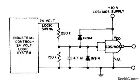
Simple resistive divider circuit provides interfacebetween 24-V logic swing of industrial controlsystem and CMOS logic operating from 10-Vsupply Filter capacitor enhances excellentnoise immunity of CMOS logic Clamp diodesensure thatinput signal voltage is between VDD and Vss-″cos/MOS Integrated Circuits'″RCA Solid State Division, Somerville, NJ, 1977, p628. (View)
View full Circuit Diagram | Comments | Reading(414)
4_DIGIT(10000_COUNT)A_D_CONVERTER
Published:2009/7/2 3:46:00 Author:May

View full Circuit Diagram | Comments | Reading(903)
400_VOLT,60_WATT_PUSH_PULL_POWER_SUPPLY_
Published:2009/7/2 3:43:00 Author:May

Circuit Notes
The design delivers a regulated 400-V, 60-W output. The TL494 switching regulator governs the opdrating frequency and regulates output voltage. R1 and C1 determine switching frequency, which is approximately 0.5RC-100 kHz for the values shown. The TL494 directly drives the FET's gates with a voltage-controlled, pulse-width-modulated signal. After fullwave rectification, the output waveform is filtered by a chokeinput arrangement. The 1 μH, 75 μF filter accomplishes the job nicely at 100 kHz. A feedback scheme using R4, R5 and R6 provides for outputvoltage regulation adjustment, with loop compensation handled by C2. Diodes D1 and D2 provide isolation and steering for the 33-V zener transient clamp, D3. Output regulation is typically 1.250/0 from noload to the full 60-W design rating. Regulation is essentially determined by the TL494. Output noise and ripple consists mainly of positive and negative 0.8-V spikes occurring when the output stage switches. (View)
View full Circuit Diagram | Comments | Reading(6787)
TTY_LINK_FOR_MICROPROCESSOR
Published:2009/7/2 3:43:00 Author:May
Demonstration circuit illustrates use of fiber-optic cable with low-cost components for relatively narrow-band application, to provide feed from remote teleprinter to microprocesson.-O. E.Marvel and J. C. Freeborn, A Little Hands-On Experience llluminates Fiber-Optic Links, EDN Magazine,Nov.5,1977,p 71-75. (View)
View full Circuit Diagram | Comments | Reading(486)
SUCCESSIVE_APPROXIMATION_A_D_CONVERTERS
Published:2009/7/2 3:42:00 Author:May

The ICL7134B-based circuit is for a bipolar-input high-speed A/D converter, using two AM25L03s to form a 14-bit successive approximation register. The comparator is a two-stage circuit with an HA2605 front-end amplifier, used to reduce settling time problerns at the summing node (see A020). Careful offset-nulling of this amplifier is needed, and if wide temperature range operation is desired, an auto-null circuit using an ICL7650 is probably advisable (see A053). The clock, using two Schmitt trigger TTL gates, runs at a slower rate for the first 8 bits, where settling-time is most critical than for the last 6 bits. The short-cycle line is shown tied to the 15th bit; if fewer bits are required, it can be moved up accordingly. The circuit will free-run if the HOLD/RUN input is held low, but will stop after completing a conversion if the pin is high at that time. A lowgoing pulse will restart it. The STATUS output indicates when the device is operating, and the falling edge indicates the availability of new data. A unipolar version can be constructed by typing the MSB (D13) on an ICL7134U to pin 14 on the first AM25L03, deleting the reference inversion amplifier A4, and tying VRFM to VRFL. (View)
View full Circuit Diagram | Comments | Reading(1767)
1_MHz_LED_PULSE_MODULATION
Published:2009/7/2 3:40:00 Author:May
Circuit provides required low driving-point impedance for fast turn-on of gallium arsenide phosphide LED used as source for high-speed pulse modulation of fiber-optic or otherlight beam. Q1 supplies DC level and modulation information to emitterfollower output stage Q3. Output current is sensed and limited to about 30 mA by Q2. Turn-on time for full brightness is 12 ns.-G.Schmidt, LED Modulator, EDN/EEE Magazine, June 15,1971,p 57. (View)
View full Circuit Diagram | Comments | Reading(482)
ZENER_GENERATOR
Published:2009/7/2 3:39:00 Author:May
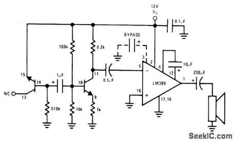
Uses National LM389 array having three transistors along with opamp. Application of reverse voltage to emitter of one grounded-base transistor breaks it down in avalanche mode to give action of zener diode. Reverse voltage characteristic, typically7.1 V, is used as noise source for amplification by second transistor and power opamp. Third transistor(notshown) can be used to gate noise generator if desired.- Audio Handbook, National Semiconductor. Santa Clara. CA. 1977. p 4-33-4-37. (View)
View full Circuit Diagram | Comments | Reading(817)
BENCH_TOP_POWER_SUPPLY
Published:2009/7/2 3:38:00 Author:May

Circuit Notes
A tapped transformer drives a diode bridge (D1-D4) and two 2500 pF filter capacitors (C1 and C2), that provide a noload voltage of 37 or 47 volts, depending upon the position of switch 52a. The unregulated dc is then fed to a pre-regulator stage composed of Q1 and D5. Those components protect IC1(the 723)from an over-voltage condition; the 723 can't handle more than 40 volts. The LED (LEDl) and its 2.2 k current-limiting resistor(R1)provide on/off indication. The current through the LED varies slightly according to the transformer tap selected, but that's of no real consequence. The series-pass transistor in IC1 drives voltage-follower Q2, providing current amplification. The transistor can handle lots of power. It has a maximum collector current of 15 amps and a maximum VCE of 70V, both of which are more than adequate for our supply. (View)
View full Circuit Diagram | Comments | Reading(2333)
MANCHESTER_CODE_DEMODULATOR
Published:2009/7/2 3:37:00 Author:May

Digital approach using ECL provides maximum speed, isselfsynchronizing for altemate bitpairs, and has minimum complexity. Developed for optically coupled 25-channel PCM telemetry system used over single optical-fiber channel.Undesired transitions in input data are masked by creating strobe. Approach recognizes distinction between identical sequences that would give some output except for time-of-occurrence restriction. Article gives step-by-step design procedure, waveforms, and excitation table.-B. R. Jarrett, Could You Design a High-Speed Manchester-Code Demodulator?,EDN Magazine,Aug.20,1974,p 75-80. (View)
View full Circuit Diagram | Comments | Reading(1016)
IR_DETECTOR
Published:2009/7/2 3:35:00 Author:May

Photodiode transforms light-signal output of fiber-optic cable to electric signal. Spectral response of detector closely matches that of IR-emitting diode at other end of cable, for maximum system efficiency. Rise and fall times of detector can be less than 35 ns when properly biased and loaded by receiver circuit. Developed by Augat, Inc.,Attleboro, MA, as part of fiber-optic evaluation kit for TTL appli cations.-Fiber-Optic Kit Allows Engineering Evaluation of Complete Interconnection System, ComputerDesign, Nov. 1977, p 27 and 30. (View)
View full Circuit Diagram | Comments | Reading(0)
COINCIDENCE_DETECTOR
Published:2009/7/2 3:34:00 Author:May

lf inputs A and B are both high, indication will be green. If A and B are both low, indication will be red. If inputs are out of phase, so one is high and the other low, indicator will be off. Suitable for monitoring complex logic circuits, Uses Monsanto MV5491 dual red/green LED, with 220 ohms in upper lead to +5 V supply and 100 ohms in lower +5 V lead because red and green LEDs in parallel back-to-back have different voltage requirements. Drivers are SN75451 and SN75454.-K. Powell, Novel Indicator Circuit, Ham Radio, April 1977, p 60-63. (View)
View full Circuit Diagram | Comments | Reading(0)
DOPPLER_BURGLAR_ALARM
Published:2009/7/2 3:34:00 Author:May

Small radar transmitter operating at 10.687 GHz fills pro-tected area with radio waves. Waves reflected from stationary objects are ignored by receiver, while waves undergoing Doppler shift in fre-quency by reflection from moving object such as intruder are selectively amplified for trigger-ing of alarm. Single waveguide section is di-vided into two cavities, each having Gunn diode; transmitter cavity feeds points A and B of transmitter TR7-IC3, and other cavity feeds points C and D of amplifier that drives alarm relay. Article covers construction and operation of circuit and gives sources (British) for parts and construction khs. Opamps are SN72748 or equivalent, IC3 is μA723 or equivalent, Tr1-Tr3 are ZTX500 or equivalent, Tr4-Tr6 are ZTX302 or equivalent, Tr7 is 3055, D1-D8 are 1N4001 or equivalent, D9-D10 are 1N914, SCR1 is TIC44 or equivalent, Z1-Z2 are BZY88-C8V2, relay is 18-V with 1K coil, Doppler module is Mullard CL8960 or equivalent, and seff-oscillating mixer for re-ceiver is Mullard CL8630S or equivalent. Alarm stays on until reset by appropriate swhch.-M.W. Hosking, Microwave Intruder Alarm, Wire-less World, July 1977, p 36-39. (View)
View full Circuit Diagram | Comments | Reading(1506)
AF_NOISE_LIMITER
Published:2009/7/2 3:33:00 Author:May

Trough limiter eliminates background noise that is normally passed by conventional limiters. to permit use of higher volume level without annoying static when monitoring single radio channel continuously,-Circuits, 73 Magazine. Dec.1973.p120. (View)
View full Circuit Diagram | Comments | Reading(726)
20_KILOBIT_FIBER_OPTIC_RECEIVER
Published:2009/7/2 3:33:00 Author:May
Phototransistor driving three-transistor amplifier provides TTL output for data rates up to 20 kilobits.- Basic Experimental Fiber Optic Systems, Motorola, Phoenix, AZ, 1978. (View)
View full Circuit Diagram | Comments | Reading(1741)
| Pages:1152/2234 At 2011411142114311441145114611471148114911501151115211531154115511561157115811591160Under 20 |
Circuit Categories
power supply circuit
Amplifier Circuit
Basic Circuit
LED and Light Circuit
Sensor Circuit
Signal Processing
Electrical Equipment Circuit
Control Circuit
Remote Control Circuit
A/D-D/A Converter Circuit
Audio Circuit
Measuring and Test Circuit
Communication Circuit
Computer-Related Circuit
555 Circuit
Automotive Circuit
Repairing Circuit