
Circuit Diagram
Index 1158
175_MHz_40_W_amplifier_28_V_supply
Published:2009/7/24 2:42:00 Author:Jessie
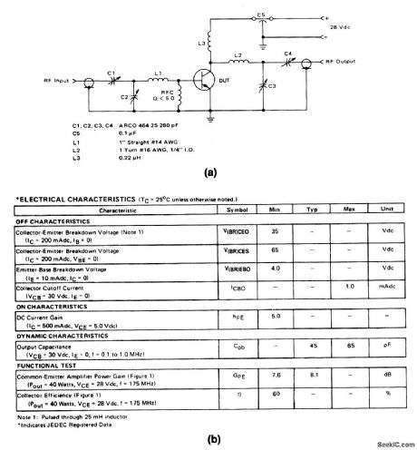
The electrical characteristics for the 2N5643 shown in this circuit are given in Fig. 2-28B. (View)
View full Circuit Diagram | Comments | Reading(865)
175_MHz_20_W_amplifier_28_V_supply
Published:2009/7/24 2:42:00 Author:Jessie
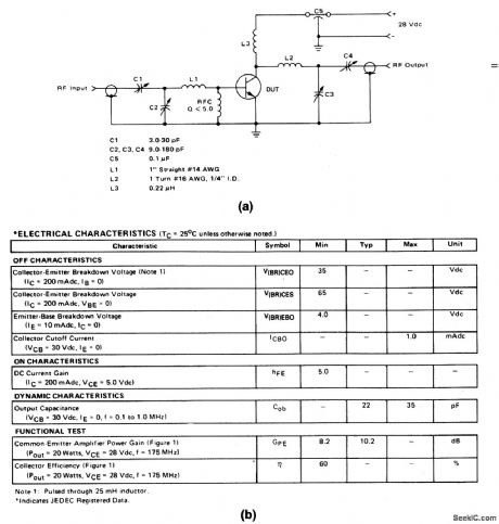
The electrical characteristics for the 2N5642 shown in this circuit are given in Fig. 2-27B. (View)
View full Circuit Diagram | Comments | Reading(759)
Temperature_to_frequency_converter
Published:2009/7/24 2:41:00 Author:Jessie

Fig. 13-24 This circuit provides a simple way to convert the current output of an LM334 temperature sensor to a corresponding output frequency. To calibrate it, place the LM334 in a 0℃environment and set the 0℃ adjustment for 0 Hz at the TTL output. Next, put the LM334 in a 100℃ environment and set the 100℃ adjust control for a 1-kHz output. Repeat this procedure until both points are fixed. This circuit has a stable 0.1℃ resolution with ±1.0℃ accuracy. Linear Technology, Linear Applications Handbook, 1990, p. AN7-2. (View)
View full Circuit Diagram | Comments | Reading(3)
UNINTERRUPTIBLE_POWER_SUPPLY_FOR_PERSONAL_COMPUTERS
Published:2009/7/2 2:05:00 Author:May


Circuit NotesThe UPS is basically an ac inverter that is powered by a 12-V, lead-acid automobile battery. During power outages, it can supply several minutes of power for an average personal computer. It incorporates a crystal-controlled 60 Hz time base, so that a computer with a real time clock can maintain its accuracy. It isolates the ac line from the computer, so it can be used to operate sensitive electronic equipment on noisy power sources.Two MTM60N06 Power FETs (Q1 and Q2) alternately switch current through a center-tapped 120-V to 12-V filament transformer (T1) with its primary and secondary reversed. The 120-V output is compared with a 60 Hz reference in a closed-loop configuration that maintains a constant output at optimum efficiency.A 60 Hz reference frequency is derived from a crystal oscillator and divider circuit, UI. An inexpensive 3.58 MHz color burst crystal provides the time base that can be accurately adjusted by C1. The 60 Hz output from U1 is applied to the exclusive-OR gate, U2, and then to the XR-2206 function generator (U3) that converts the square wave into a she wave. U2 and U3 form a phase-locked loop that synchronizes the sine wave output o f U3 with the 60 Hz square wave reference of U1. The she wave is then inverted by op amp U4a, so that two signals 180 out of phase can be applied to U4b and U4c that drive Q1 and Q2. Due to the closed-loop configuration of the drive circuits, Q1 and Q2 conduct only during the upper half of the sine wave. Therefore, one TMOS device conducts during the first half of the sine wave and the other conducts during the second half. (View)
View full Circuit Diagram | Comments | Reading(4925)
CLAPP_JFET_VFO
Published:2009/7/24 2:41:00 Author:Jessie
The JFET VFO circuit shown here can be identified as a Clapp oscillator by its series-tuned LC network. This circuit as shown can be used from 0.5 to 7 MHz. (View)
View full Circuit Diagram | Comments | Reading(740)
DATA_COUPLER_WITH_ISOLATION
Published:2009/7/2 2:04:00 Author:May

Length of fiber or polystyrene rod determines amount of voltage isolation provided between digital or analog signal input and Fairchild FPT 100 photodetector driving Optical Electronics 9720 opamp having 100-mA output for driving cables, relays, or loudspeakers. LED can be Monsanto MV50 handling up to 200 mA. Output of opamp is zero for no light. Pulse-duration modulation should be used for transmission of analog data.- High Voltage Optically Isolated Data Coupler, Optical Electronics, Tucson, AZ,Application Tip 10266. (View)
View full Circuit Diagram | Comments | Reading(704)
AM_NOISE_SILENCER
Published:2009/7/2 2:02:00 Author:May

Circuit samples mixer output (IF input) of AM receiver and, when noise pulse is detected, interrupts IF input signal for duration of noise pulse. Uses National LM372IC having AGC loop with range of about 69 dB, for accommodating wide range of input levels. Artide describes operation of circuit in detail. For frequencies above 2 MHz, use LM373 in place of LM372.-T. A. Tong, Noise Silencer torA.M. Receivers, Wireless World. Oct. 1972. p 483-484. (View)
View full Circuit Diagram | Comments | Reading(963)
AF_POWERED_CLIPPER
Published:2009/7/2 1:56:00 Author:May

Designed for use just ahead of 8-ohm loudspeaker in receiver covering lower amateur phone bands (75 and 40 me-ters). Reduces hissing noise caused by shortwave diathermy, electric motors, and fluorescent lighting, as well as impulse noise generated by auto ignition system or atmospheric interference. T1 and T2 are transistor radio output transformers with 500:4 or 600:8 ohm impedance. Q1 is 2N2222 NPN transistor. Q2 is 2N29O7 PNP transistor. D1 and D2 are 1N270.-C. Laster. An Audio Powered Noise Clipper. CQ. May 1976. p 26-27. (View)
View full Circuit Diagram | Comments | Reading(2321)
JOYSTICK_CONTROL
Published:2009/7/2 1:45:00 Author:May

Mechanically conttolled voltage source generates two independent con-trol voltages, proportional to stick position, to serve as one of controls for elaborate sound synthesizer used for generating wide variety of musical and other sounds. Three-part article describes circuit operation and gives all other circuits used in synthesizer.-T. Ort and D. W. ThomasElectronic Sound Synthesizer, wireless world Part 3-Oct 1973.p 485-490(Part1-Aug 1973.p 366-372;Part 2-Sept.1973.p429-434) (View)
View full Circuit Diagram | Comments | Reading(788)
175_MHz_25_W_amplifter_125_V_supply
Published:2009/7/24 2:58:00 Author:Jessie
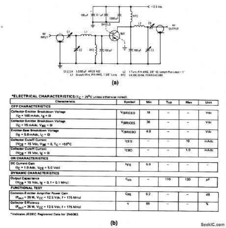
The electrical characteristics for the 2N6082 shown in this circuit are given in Fig.2-35B. (View)
View full Circuit Diagram | Comments | Reading(1794)
Oven_temperature_controller_with_RTD_sensor
Published:2009/7/24 2:57:00 Author:Jessie

Fig. 13-34 This circuit is similar to that of Fig, 13-27, except that the sensor is a platinum RTD. If the sensor is in close thermal contact with the heater, the circuit will easily control to 0.1℃ stability over widely varying ambient temperatures. National Semiconductor, Linear Applicatrions Handbook 1991 p 858.
(View)
View full Circuit Diagram | Comments | Reading(1382)
STAIRCASE_COUNTER
Published:2009/7/24 2:57:00 Author:Jessie
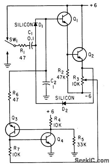
Q1-Q2 serve as boot-strap amplifier for voltage on storage capacitor C2. Each incoming pulse transfers charge increment from C1 to C2. Reliable counts as large as Ion are easily obtained.-N. C. Hekimian, PNP-NPN CIRCUITS: New Look at a Familiar connection, Electronics, 35:47, p 42-46. (View)
View full Circuit Diagram | Comments | Reading(516)
8_AMP_REGULATED_POWER_SUPPLY_FOR_OPERATING_MOBILE_EQUIPMENT
Published:2009/7/2 1:45:00 Author:May

Circuit Notes
This supply is powered by a transformer operating from 120 Vac on the primary and providing approximately 20 Vac on the primary, and providing approximately 20 Vac on the secondary. Four 10-A diodes with a 100 PIV rating are used in a full-wave bridge rectifier. A 10,000 μF/36 Vdc capacitor completes the filtering, providing 28 Vdc. The dc voltage is fed to the collectors of the Darlington connected 2N3055's, Base drive for the pass tfansistors is from pin 10 of the μA723 through a 200 ohm current limiting resistor, R1. The reference terminal (pin 6) is tied directly to the noninverting input of the error amplifter (pin 5), providing 7.15 V for comparison.
The inverting input to the error amplifier(pin 4) is fed from the center arm of a 10 k ohm potentiometer connected across the output of the supply. This control is set for the desired output voltage of 13.8 V. Compensation of the error amplifier is accom-plished with a 500 pF capacitor connected from pin 13 to pin zL. If the power supply should exceed 8 A or develop a short circuit, the μA723 regulator will bias the transistors to cutoff and the output voltage will drop to near zero until the short circuit condition is corrected.
(View)
View full Circuit Diagram | Comments | Reading(832)
WIDE_RANGE_STAIRCASE_GENERATOR
Published:2009/7/24 2:57:00 Author:Jessie
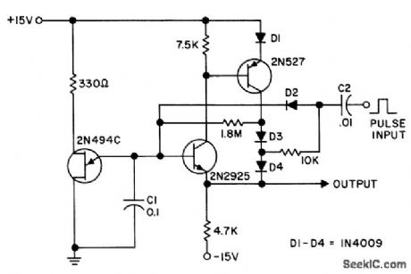
Has high input impedance und low output impedance, to reduce droop in output voltage between pulses. Staircase is generated by pump D2-C2, which is boostrapped on output to maintain equal amplitude on each step. Circuit values shown give 10 steps with 12-V input pulse.- Transistor Manual, Seventh Edition, General Electric Co., 1964, p 345. (View)
View full Circuit Diagram | Comments | Reading(805)
THEREMIN
Published:2009/7/2 1:40:00 Author:May

Two transistor oscillator stages generate separate low-power RF signal in broadcast band, for pickup by AM broadcast receiver. Movement of hand toward or away from metal pitch plate varies trequency of Q1, making audio output of receiver vary conespondingly as beat frequency changes. Both circuits are Hartley oscillators, using Miner 9012 or equivalent slug-tuned colls. To adjust initially, place next to radio and set tuning slug of L1 about two-thirds out of its winding. Set slug of L2 about one-third out of its winding. Tune radio until either oscillator signal is heard. Signal can be identified by whistle if on top of broadcast station or by quieting of background noise if between stations. Adjust slugs so whistle is heard at desired location ot quieting signal. Pitch of whistleshould change now ashand is brought near pitch plate.-J. P Shields, How to Build Proximity Detectors & Metal Locators, Howard W. Sams, Indianapolis, IN, 2nd Ed. 1972. p 154-156. (View)
View full Circuit Diagram | Comments | Reading(2951)
175_MHz_15_W_amplifier_125_V_supply
Published:2009/7/24 2:56:00 Author:Jessie

The electrical characteristics for the 2N6081/MRF221 shown in this circuit are given in Fig.2-34B. (View)
View full Circuit Diagram | Comments | Reading(1150)
HAND_WAVING_THEREMIN
Published:2009/7/2 1:31:00 Author:May
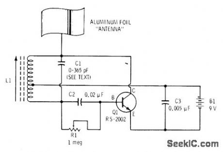
Single-transistor RF oscillator is tuned to generate frequency about 455 kHz above oscillator frequency of transistor radio. With aluminum-foil antenna away from nearby objects and radio tuned be-tween stations, R1 is adjusted until highpitched tone is heard from radio. Now, as hand is brought toward and away from foil antenna, wailing sounds are produced. With practice, musician can produce recognizable melodies by vibrating hand. Primary controls of frequency are C1 (10-365 pF broadcast radio tuning capacitor) and adjustable antenna coil L1 (Radio Shack 270-1430). Radio can be up to 15 feet away from theremin. Rotate radio for maximum pickup from L1-F. M. Mims, Electronic Music Projects, Vol. 1, Radio Shack, Fort Worth, TX, 1977, 2nd Ed. p 81-89. (View)
View full Circuit Diagram | Comments | Reading(1621)
POWER_AMPLIFIER
Published:2009/7/2 1:23:00 Author:May


Circuit NotesFor most applications, the available power from op amps is sufficient. There are times when more power handling capability is necessary. A simple power booster capable of driving moderate loads uses an NE5535 device. Other amplifiers may be substituted only if R1 values are changed because of the ICC current required by the amplifier.R1 should be calculated from the expression (View)
View full Circuit Diagram | Comments | Reading(1602)
Temperature_to_pulse_width_converter
Published:2009/7/24 2:54:00 Author:Jessie

Fig. 13-33 This circuit uses an LM3524 pulse-width modulator to convert the output of an LM135 temperature transducer into a pulse width that can be measured by a digital system (such as a microprocessor-based data-acquisition system). Although the example uses the temperature transducer as the input, the circuit will convert any 0.1- to 5-V input applied to the 100-kΩ resistor into a 0- to 500-ms output pulse width with 0. 1 % linearity. The overall temperature-to-pulse-width scale factor is adjusted with the 5-kΩ gain-trim potentiometer. The oscillator output pulse at pin 3 of the LM3524 (not shown) occurs just before the pins 11/14 output pulse and it can be used to reset counters or other digital circuits. National Semiconductor Linear Applications Handbook, 1991, p 857. (View)
View full Circuit Diagram | Comments | Reading(776)
440__to_480_MHz_broadband_UHF_amplifier_125_V_supply
Published:2009/7/24 2:54:00 Author:Jessie
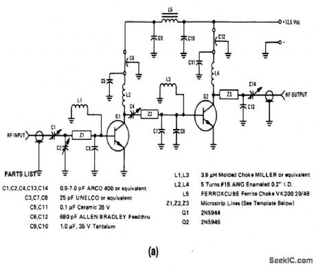


The electrical characteristics for the 2N5944 and 2N5946 shown in this circuit are given in Fig. 2-33B. Figures 2-33C and 2-33D show the amplifier performance over the frequency range. Figures 2-33E and 2-33F show the PC-board photomaster, and parts placement, respectively. Those not familiar with microstrip techniques (for Z1, Z2, and Z3) should read the many Motorola Publications, such as AN548A and AN555. (View)
View full Circuit Diagram | Comments | Reading(1003)
| Pages:1158/2234 At 2011411142114311441145114611471148114911501151115211531154115511561157115811591160Under 20 |
Circuit Categories
power supply circuit
Amplifier Circuit
Basic Circuit
LED and Light Circuit
Sensor Circuit
Signal Processing
Electrical Equipment Circuit
Control Circuit
Remote Control Circuit
A/D-D/A Converter Circuit
Audio Circuit
Measuring and Test Circuit
Communication Circuit
Computer-Related Circuit
555 Circuit
Automotive Circuit
Repairing Circuit