
Circuit Diagram
Index 1140
Voltage_boosted_output_op_amp
Published:2009/7/24 2:03:00 Author:Jessie

This 1.5-V powered amplifier provides 0 to 10 V outputs at up to 75-μA capacity. With the values shown, voltage gain is about 100. Gain can be increased provided that the 1.5-V powered LM10 common-mode input not be exceeded. (View)
View full Circuit Diagram | Comments | Reading(592)
GO_NO_GO_VTVM
Published:2009/7/24 2:03:00 Author:Jessie

For applications in which voltage with specified tolerance must be monitored by unskilled production-line personnel. Three lamps indicate voltage. Go band can be as narrow as 0.1 v. Basic range of 100 v can be extended with dividers.-A Go No-Go Vacuum Tube Voltmeter, Electronic Circuit Design Handbook, Mactier Pub. Corp., N.Y., 1965, p 156. (View)
View full Circuit Diagram | Comments | Reading(622)
PHOTOCELL_CHOPPER
Published:2009/7/24 2:02:00 Author:Jessie

Allows millivolt d-c voltages to be measured accurately with ordinary average-reading vtvm. Neon lamps are fired alternately by rectified 60-cps line voltage, causing Clairex photocells to alternate between low und high resistance states and thereby chop d-c input voltage being measured.-I. Queen, Chopper Adapts Voltmeter to D-C, Electronics, 38:22, p 66-67. (View)
View full Circuit Diagram | Comments | Reading(764)
TRANSFO_RM_ER_CONTROLLED_SHIFT_REGISTER
Published:2009/7/24 2:02:00 Author:Jessie

Can be built to shift forward, backward, or in n dimensions. With series of flip-flops, stored information can be rearranged arbitrarily, in single pulse.-W. M. Carey, Using Inductive Control in Computer Circuits, Electronics, 32:38, p 31-33. (View)
View full Circuit Diagram | Comments | Reading(599)
PASS_REJECT_TUNABLE_NOTCH
Published:2009/7/2 9:16:00 Author:May
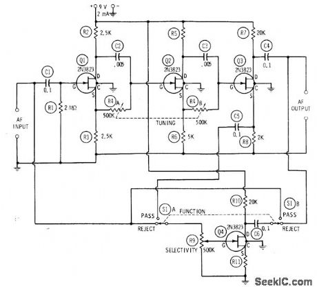
Full rotation of ganged tuning control R4 tunes circuit from 100 Hz to 10 kHz, with position of switch S1 determining whether circuit passes or rejects frequency to which it is tuned. Maximum selectivity, conesponding to maximum height of pass curve or depth of reject curve and minimum width of either curve, is obtained when R9 is set for maximum gain in FET Q4. If R9 is advanced far enough with switch set to pass, circuit will oscllate and give sine-wave output at tuned frequency.-R.P.Tumer, FET Circuits, Howard W, Sams, Indianapolis, IN, 1977, 2nd Ed., p 71-73. (View)
View full Circuit Diagram | Comments | Reading(520)
PRECISION_VFO
Published:2009/7/2 9:15:00 Author:May

Permeability-tuned oscillator provides stability and linearity at low cost for receivers with 160-meter tunable IF stages. L1 has 28 turns No. 36 enamel closewound on J. W. Miller form 64A022.2. Article covers construction of tuning dial, incuding contouring of L1 core to give good dial linearity. Frequency coverage is 2.255-2.509 MHz. Direct-reading dial is accurate within 1.5 kHz over entire 250-kHz tuning range.-W. A. Gregoire, Jr., A Permeability-Tuned Variable-Frequency Oscillator, QST, March 1978, p 26-28. (View)
View full Circuit Diagram | Comments | Reading(2123)
FLIP_FLOP_BUILDING_BLOCKS
Published:2009/7/24 2:02:00 Author:Jessie

Inductively coupled flip-flops are put together to form shift register. Both signal and shift pulses are positive. Operates reliably over wide ranges of input pulse amplitude and circuit parameters.-M. M. Perugini and N. Lindgren, Recent Progress in Solid State Technology, Electronics, 33:10, p 39-43. (View)
View full Circuit Diagram | Comments | Reading(609)
20_500_kHz_CRYSTAL
Published:2009/7/2 9:15:00 Author:May

Series-mode oscillator requires no tuned circuit, gives choice of sine or square output, and has good frequency and mode stability. Works nicely with troublesome FT241 crystals. If any crystal fails to start reliably, increase R1 to 270 ohms and R2 to 3.3K. For squire-wave operation, C1 is 1-μF nonelectrolytic. Omit C1 for sine-wave operation; harmonic output is then quite low, whh second harmonic typically -30 dB. Output is about 1.5-VRMS sine wave or 4-V square wave.-R. Harrison, Survey of Crystal Oscillators, Ham Radio, March 1976, p 10-22. (View)
View full Circuit Diagram | Comments | Reading(1386)
2_A_5_A_step_doryn_PWM_regulators
Published:2009/7/24 2:02:00 Author:Jessie


Figure 7-48 shows an LT1076 connected to provide an output of +5 V at 2 A, with an input of 10 V to 40 V. Figure 7-49 shows an LT1074 connected to provide an output of +5 V at 5 A, with an input of 10 V to 40 V. Both ICs have a quiescent current of 8.5 mA. MAXIM NEW RELEASES DATA BOOK, 1994, P. 4-251, 4-254. (View)
View full Circuit Diagram | Comments | Reading(1515)
SCS_SHIFT_REGISTER
Published:2009/7/24 2:01:00 Author:Jessie

Shill pulse turns off all silicon controlled switches. Trailing edge of turnoff pulse is differentiated for turning on appropriate stages. 2N2714 will easily drive ten scs stages.- Transistor Manual, Seventh Edition, General Electric Co., 1964, p 432. (View)
View full Circuit Diagram | Comments | Reading(617)
VOLTAGE_CONTROLLED_BANDPASS
Published:2009/7/2 9:14:00 Author:May

Two Optical Electronics S898 four-quadrant analog multipliers and 3704 state-variable active filter permit use of voltage control for changing filter characteristics remotely without having noise pickup problems on control Iines. Analog multipliers serve as variable-gain blocks that change cument levels in resistors and in effect change resistor values. Circuit has Iinear relationship of frequency to control voltage, constant gain andQwith frequency, and good temperature stability.- Voltage-Controll ed Active Bandpass Filter, Optical Electronics, Tucson, AZ, Application Tip 10269. (View)
View full Circuit Diagram | Comments | Reading(651)
50_500_kHz_CRYSTAL
Published:2009/7/2 9:13:00 Author:May

Parallel-mode low-frequency oscillator makes excellent BFO for 455 kHz. If oscillator will not start, reduce value of feedback resistor RF. Increasing RF reduces harmonic output, but oscillator may then take up to 20 s to reach full output. For crystals with specified load capacitance of 30 or 50 pF, remove 100-pF capacitor C1 in series with crystal. Q1 is 2N2920, 2N2979, 2N3565, 2N3646, 2N5770, BC107, or BC547.-R. Harrison, Survey of Crystal Oscillators, Ham Radio, March 1976, p 10-22. (View)
View full Circuit Diagram | Comments | Reading(4590)
ESD_protected_transceivers_5_V
Published:2009/7/24 2:01:00 Author:Jessie


Figure 3-27 shows the typical application circuits and pin configurations for the MAX202E,232E. Figure 3-28 shows the MAX211E, 213E, 241E. These ICs are designed to operate in harsh environments, but still meet EIA/TIA-232E specifications. Each transmitter output and receiver input is protected against ±15-kV electrostatic discharge (ESD). MAXIM NEW RELEASES DATA Book 1995, P.2-54, 2-55. (View)
View full Circuit Diagram | Comments | Reading(581)
DC_LEVEL_SHIFTER_FOR_AF
Published:2009/7/2 9:13:00 Author:May

Circuit using optical Electronics 9803 opamps separates AF input signal into two outputs. Low-pass output contains DC to 10 Hz, and high-pass output has frequency content above 10 Hz to upper frequency limit approaching 10 MHz for opamp used. Dynamic output impedance of both outputs is less than 1 ohm. Both outputs have DC continuity. DC output of high-pass terminal is equal to offset voltage of integrator. DC output of low-pass terminal equals DC input plus offset voltages of both opamps.- Automatic DC Level Shifter, Optical Electronics, Tucson, AZ, Application Tip 10226. (View)
View full Circuit Diagram | Comments | Reading(940)
BALANCED_VTVM
Published:2009/7/24 2:01:00 Author:Jessie

V1 operates at low plate current to keep grid current small; V2 operates normally to drive meter circuit. R1 is switched for voltage ranges. Chief drawback is that aging of tubes increases their output resistances, making meter read low.-J. J. Faran Jr., Hybrid Voltmeter Avoids Aging Errors, Electronics, 36:38, p 41. (View)
View full Circuit Diagram | Comments | Reading(658)
48_MHz
Published:2009/7/2 9:12:00 Author:May

Uses all four sections of 7400 quad dual-input NAND gate to give 4.8 MHz output at pin 8, as harmonic-rich square wave. Can cause severe television interference during testing. Article gives five other crystal oscillator circults using same IC.-A. MacLean, How Do You Use ICs?, 73 Magazine, Oct. 1976, p 38-41. (View)
View full Circuit Diagram | Comments | Reading(1119)
7_MHz
Published:2009/7/2 9:12:00 Author:May

Uses single Siliconix 2N2608 FET. Keep leads short. Coil can be air-wound or permeability-tuned. If tuning capacitor is variable, coil value can be fixed. RF output level depends on circuit voltages and on activity of crystal used.-Q & A, 73 Magazine, April 1977, p 165. (View)
View full Circuit Diagram | Comments | Reading(892)
MODULATED_CRYSTAL
Published:2009/7/2 9:11:00 Author:May

CA3000 differential amplifier is operated as efficient crystal-controlled oscillator. Output frequency depends on crystal. If desired, RF output can be modulated with low-frequency tone applied between pin 2 and ground.-E. M. Noll, Linear IC Principles, Experiments, and Proiects, Howard W. Sams, Indianapolis, IN, 1974, p 91. (View)
View full Circuit Diagram | Comments | Reading(909)
1_MHz_WITH_ONE_GATE
Published:2009/7/2 9:10:00 Author:May
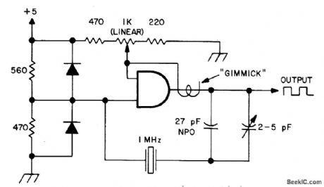
Crystal oscillator uses only onesection of SN7408 TTL quad AND gate. Use series-resonant crystal having 30-pF series capacitance. Adjust 1K pot for reliable start-up and symmetrical square-wave output. Diodes are 1N34A or 1N914. Gimmick is 1 or 2 turns of insulated wire wrapped around output lead.-Clyde E. Wade, Jr., An Even Simpler Clock Oscillator, 73 Magazine, Nov./Dec. 1975, p 164. (View)
View full Circuit Diagram | Comments | Reading(714)
LOW_NOISE_5_MHz
Published:2009/7/2 9:09:00 Author:May
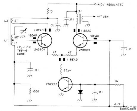
Very low-noise high-QLC oscillator operating at 5 MHz is designed for use in high-performance communication receivers. Oscillator uses two stages, one oporating in class A and the other operating as limiter that also serves as feedback path.-U. L. Rohde, Effects of Noise in Receiving Systems, Ham Radio, Nov. 1977, p 34-41. (View)
View full Circuit Diagram | Comments | Reading(535)
| Pages:1140/2234 At 2011211122112311241125112611271128112911301131113211331134113511361137113811391140Under 20 |
Circuit Categories
power supply circuit
Amplifier Circuit
Basic Circuit
LED and Light Circuit
Sensor Circuit
Signal Processing
Electrical Equipment Circuit
Control Circuit
Remote Control Circuit
A/D-D/A Converter Circuit
Audio Circuit
Measuring and Test Circuit
Communication Circuit
Computer-Related Circuit
555 Circuit
Automotive Circuit
Repairing Circuit