
Circuit Diagram
Index 1122
15_A_negative_fixed_voltage_regulator
Published:2009/7/23 23:43:00 Author:Jessie

The LAS1800 series voltage regulators are ICs that contain all elements necessary for linear regulation (safe-area protection, thermal overload, current limiting, as shown in Fig. 7-42C). Figure 7-42B shows the output voltage and tolerance for the various LAS1800 part numbers. Figure 7-42D shows the absolute maximum ratings. (View)
View full Circuit Diagram | Comments | Reading(696)
PREFERRED_AMPLIFICATION_300_PREAMPLIFIER
Published:2009/7/23 23:43:00 Author:Jessie

Used with instrument servo motor controller to increase available gain. Chopper is used with d.c inputs only.-NBS, Handbook Preferred Circuits Navy Aeronautical Electronic Equipment, Vol. I, Electron Tube Circuits, 1963, PC 73, p 73-2. (View)
View full Circuit Diagram | Comments | Reading(617)
ESUBX_SUB_transfer_function_V_F_converter
Published:2009/7/23 23:43:00 Author:Jessie

Fig. 12-15 This circuit responds exponentially to the input voltage and is ideally suited for electronic music synthesizers. The circuit has a 1-V-in/octave-offrequency-out scale factor, with exponential conformity with 0.13% over a 10-Hz to 20-kHz range, and 150 ppm/℃ drift. Both a pulse output and a ramp output are available (the ramp is used where substantial power at the fundamental frequency is required). To trim, ground the Q3 base and adjust the 2-kΩ potentiometer so that the A3 inverting input is 100 mV above the noninverting input. Remove the ground at Q3. Linear Technotogy Linear Applications Handbook 1990, p AN14-15. (View)
View full Circuit Diagram | Comments | Reading(579)
Step_down_PWM_switch_mode_regulators
Published:2009/7/23 23:43:00 Author:Jessie


Figure 7-17 shows the MAX724/26 connected as basic step-down converters,Figures 7-18 and 7-19 show the pin configurations.Figure 7-20 shows component suppliers.MAXIM EVALUATION KIT DATA Book, 1994, P. 3-131, 3-131, 3-139. (View)
View full Circuit Diagram | Comments | Reading(656)
TRIODE_COMMON_PLATE_MIXER
Published:2009/7/23 23:43:00 Author:Jessie
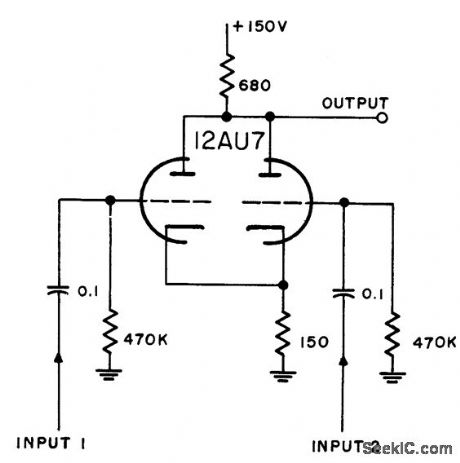
Is good adder for coincident inputs. Proves unity gain. Generally preferred to pentode common-plate mixers.-NBS, Handbook Preferred Circuits Navy Aeronautical Electronic Equipment, Vol. 1, Electron Tube Circuits, 1963, p N4-8. (View)
View full Circuit Diagram | Comments | Reading(834)
DACs_with_high_voltage_and_high_current_outputs
Published:2009/7/25 5:37:00 Author:Jessie

Figure 9-38 shows DAC1006s connected for high-voltage outputs, both unipolar and bipolar. The output current of these circuits depends on the current limit of the LM143 op amp (typically 20 mA). Figure 9-39 shows how a discrete power stage can be added to further increase output current capability (to 100 mA at 100 V). NATIONAL SEMICONDUCfOR, APPLICATION NOTE 271, 1994, P. 668. (View)
View full Circuit Diagram | Comments | Reading(659)
Capacitance_multiplier
Published:2009/7/25 5:35:00 Author:Jessie

Figure 9-37 shows a DAC0830 connected as a capacitance multiplier,Actually, thecircuit is a DAC-controlled amplifier (used for capacitance multiplication) to give microprocessor control of system time-domain or frequency-domain response. The microprocessor controls the digital input to the DAC、which controls the amplifier to produce a variable capacitance,The capacitance can be used to varythe time constant of RC circuits varying either time or frequency.In this circuit the DAC adjusts the gam of a stage with fixed capacitive feedback. This produces aMiller-effect equivalent input capacitance equal to the fixed capacitance multiplied by 1 plus the amplifier gain.The voltage across the equivalent input capacitance to ground is limited to the maximum output voltage of op amp A1, divided by 1 plus 2n/D, where:n = the DAC bits of resolution, and D = decimal equivalent of the binary input. NATIONAL SEMICONDUCTOR, APPLICATION NOTE 271, P. 667.
(View)
View full Circuit Diagram | Comments | Reading(4367)
Decoded_Z80_interface
Published:2009/7/25 5:10:00 Author:Jessie

Figure 9-23 shows the ADC0816/17 connected to form a decoded 280 interface. A 6-bit comparator is used to decode A4 through A7 and IOREQ Two NOR gates are used to gate the ALE/START and OE pulses. This configuration functions the same as that of Fig. 9-22, except that the DM8131 provides much more decoding. NATIONAL SEMICONDUCTOR, APPLICATION NOTE 258, 1994, P. 608.
(View)
View full Circuit Diagram | Comments | Reading(634)
Comparator_logic_level_translator_TTL_to_CMOS
Published:2009/7/24 4:52:00 Author:Jessie

Fig. 15-32 This circuit shows two sections of an HA-4900 used as a TTL to CMOS interface. Additional sections can be added. Negative logic devices may also be interfaced with appropriate supply connections, If separate supplies are used for V- and YLOGIC-, this circuit will tolerate several volts of ground-line differential noise. Figures 15-32B and 15-32C show the pin connections, and electrical characteristics, respectively. Harris Semiconductor Linear & Telecom ICs, 1991 p, 4-24 4-25, 4-29. (View)
View full Circuit Diagram | Comments | Reading(735)
PEAK_VOLTMETER_FOR_NARROW_PULSES
Published:2009/7/24 0:01:00 Author:Jessie

Addition of dual-triode amplifier V2 to conventional peak voltmeter reduces charging time constant while increasing available time for measuring peak value. Linearity is good up to 40 v.-M. Uno, Amplifier Improves Peak Voltmeter Response, Electronics, 37:14, p 73. (View)
View full Circuit Diagram | Comments | Reading(690)
Low_voltage_compandor
Published:2009/7/24 0:01:00 Author:Jessie

This single-chip circuit operates on voltages from 3 V to 7V, with a reference voltage (pin 8) of 100 mV for 0 dB. There is one dedicated summing op amp per channel, and two extra uncommitted op amps. The output can drive 600Ω. (View)
View full Circuit Diagram | Comments | Reading(1157)
ON_OFF_RELAY_SERVO
Published:2009/7/24 Author:Jessie

Step-function potentiometer provides on-off characteristic of null detector. Easily adjusted damping is applied through differential relay contacts to eliminate oscillations. Fast response to small angular displacements assures dose following. Tapping positive voltage off stop-function potentiometer causes current low through Q1, operation of relay K1A, and upward movement of arms. Negative voltage moves arms downward, reversing motor travel.-S. Shenfeld, Transistors Reduce Relay Servo Size, Electronics, 31:33, p 74-77. (View)
View full Circuit Diagram | Comments | Reading(891)
TWO_SPEED_SERVO
Published:2009/7/23 23:56:00 Author:Jessie

Directly drives size 11 motor, eliminating need for output transformer. Zener diodes provide switching between fine and coarse signals for two speeds. Maximum coarse and One signal input is 26 V rms at 400 cps. Voltage gain of coarse amplifier Q1 is 25, and gain of feedback amplifier Q2-Q3-Q4-Q5 is 460.-B. E. Orr, Direct Drive Amplifier for Two-Speed Servos, Electronics, 31:11, p 146-147. (View)
View full Circuit Diagram | Comments | Reading(712)
8_A_positive_fixed_voltage_regulator_with_remote_sensing
Published:2009/7/23 23:56:00 Author:Jessie

This circuit uses the LAS3905 IC (Fig.7-50) as a voltage regulator with remote sensing. Characteristics are shown in Fig.7-50B, 7-50C, and 7-50D. (View)
View full Circuit Diagram | Comments | Reading(777)
RANGE_STROBE_MARKER_IFF_MIXER
Published:2009/7/23 23:55:00 Author:Jessie
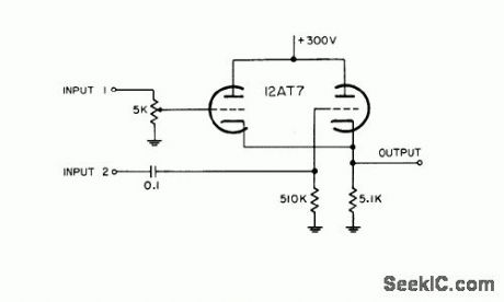
Combines positive-polarity markers with iff signals, to give 8-v positive output.-NBS, Handbook Preferred Circuits Navy Aeronautical Electronic Equipment, Vol. 1, Electron Tube Circuits, 1963, p N4-2. (View)
View full Circuit Diagram | Comments | Reading(811)
Single_chip_audio_amplifier_BTL_stereo_3_W
Published:2009/7/24 Author:Jessie
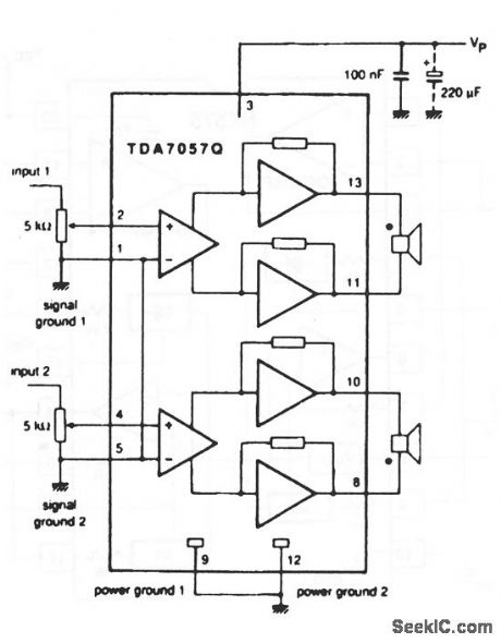
This circuit is similar to that of Fig. 1-27, except that no built-in volume control is provided, and two (stereo) channels are available. The supply range is from 3 V to 18 V. The circuit provides a 3-W per channel output, with an 11-V supply, into 16-Ω loads. Fixed, closed-loop voltage gain is 39 dB (1-V supply, 16-Ω load). (View)
View full Circuit Diagram | Comments | Reading(1029)
D_C_VOLTAGE_COMPARATOR
Published:2009/7/24 Author:Jessie

Compares long-duration sawtooth input with d-c reference and generates pulse when inputs coincide.-R. D. Valentine, D-C Voltage Comparator Circuit Uses Tube and Transistor, Electronics, 34:24, p 66. (View)
View full Circuit Diagram | Comments | Reading(652)
Negative_output_F_V_converter
Published:2009/7/24 Author:Jessie

Fig. 12-24 This circuit is similar to that of Fig. 12-19, but with an output/buffer op amp connected to provide a negative output voltage. The 1-MΩ offset adjust can be set to accommodate variations in supply voltage (with 0-V output for a grounded or 0-Hz input). Because the offset voltage is taken from the stable 1.9-V reference voltage from pin 2 of the LM331, any supply-voltage shifts cause no output shifts. Although 1-MΩ is shown, the offset potentiometer can have any value between 200 kΩ and 2 MΩ. The optional bypass capacitor C2 (across R5) prevents output noise arising from stray noise pickup at the noninverting input of the op amp. To trim, set the 5-kΩ gain-adjust control for -10-V output with a 10-kHz input. National Semiconductor Linear Applications Handbook 1991 p 1302. (View)
View full Circuit Diagram | Comments | Reading(670)
PREFERRED_RESOLVER_DRIVER
Published:2009/7/23 23:59:00 Author:Jessie

A-c operational amplifier is used as isolation amplifier, employing feedback that includes compensating winding of a-c resolver being driven. Useful as computing element for coordinate conversion, coordinate rotation, and resolution of vectors when accuracy of 0.5% is sufficient. Component values given are for 500 cps, with Mark 4 Mod 0 resolver.-NBS, Handbook Preferred Circuits Navy Aeronautical Electronic Equipment, Vol. I, Electron Tube Circuits, 1963, PC 79, p 79-2. (View)
View full Circuit Diagram | Comments | Reading(706)
_5_V_to_±12_V_±15_V_converter_module
Published:2009/7/23 23:59:00 Author:Jessie


Figure 7-27 shows a MAX1743 3-W converter module that requires no external components. The module supplies 125 mA at 112 V or 100 mA at 115 V. Pin strapping selects 112-V or 115-V operation. Figure 7-28 shows the pin descriptions and operating characteristics. Figure 7-29 shows an optional stand-by mode circuit. MAXIM NEW RELEASES DATA Book, 1994, P. 4-27, 4-29, 4-30.
(View)
View full Circuit Diagram | Comments | Reading(578)
| Pages:1122/2234 At 2011211122112311241125112611271128112911301131113211331134113511361137113811391140Under 20 |
Circuit Categories
power supply circuit
Amplifier Circuit
Basic Circuit
LED and Light Circuit
Sensor Circuit
Signal Processing
Electrical Equipment Circuit
Control Circuit
Remote Control Circuit
A/D-D/A Converter Circuit
Audio Circuit
Measuring and Test Circuit
Communication Circuit
Computer-Related Circuit
555 Circuit
Automotive Circuit
Repairing Circuit