
Circuit Diagram
Index 1130
SIGAIAL_CONDITIONER
Published:2009/7/2 22:52:00 Author:May
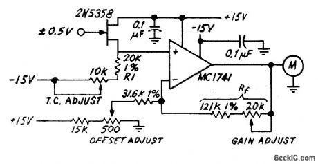
FET-buffered opamp circuit will operate from source impedances up to 100 megohms while providing voltage gain of 5. Offset adjustment is provided forinitial calibration of circuit. Developed for use with highimpedance sensors such as pH electrodes.- Industrial Control Engineering Bulletin. Motorola. Phoenix. AZ. 1973. EB-4. (View)
View full Circuit Diagram | Comments | Reading(545)
AUTOMATIC_SEARCH_AND_CONTROL
Published:2009/7/24 1:35:00 Author:Jessie

Used in servo control systems when automatic acquisition and linear search are desired, as in aid and phase-lock controls. Basic circuit was used in phase-lock microwave sys terns having 300-kc bandwidth. Active integrator is used as linear search generator as well as control system integrator.-W. H. Schuette, Automatic Search and Control Circuit for Servo Loop, EEE, 12:11, p 67-68. (View)
View full Circuit Diagram | Comments | Reading(564)
AUDIBLE_CMOS_PROBE
Published:2009/7/2 22:51:00 Author:May
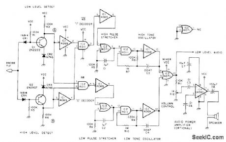
Eliminates need for watching meterwhile applying probe tip in turn to large number of closely spaced terminals during troubleshooting. Produces high tone for logic high, low tone for logic low, and no sound for open or floating string. Supplyis 12V.Articledescribes circuit operation in detaiL-C. W. An-dreasen, The Best Probe Yet?, 73 Magazine, April 1978, p 134-135. (View)
View full Circuit Diagram | Comments | Reading(559)
TTL_PROBE
Published:2009/7/2 22:46:00 Author:May


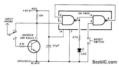
LED comes on, and stays on until circuit is reset, if input probe receives low-level (negative-going) pulse when polarity switch is set as shown. For other position of switch, LED comes on for high-level or+5 V pulse,-R .BShreve,Troubleshooting Logic Circuits,HamRadio.Feb 1977,p 56-59, (View)
View full Circuit Diagram | Comments | Reading(586)
144_MHz_FM_TRANSMITTER_
Published:2009/7/2 22:43:00 Author:May

Low-power circuit was developed for use with double-conversion continuous-tuning FM receiver suitable for either fixed or mobile communication on 2-meter amateur band. Q4-Q6 are part of RCA CA3018 IC. Power output with 12-V supply is about 1.5 VV. Two crystals are selected by slide switch; tuning can be compromised to use crys-tals whose 2-meter outputs are 1 MHz apart.Article also gives all circuits for receiver.-J. H.Ellison, Compact Package for Two-Meter FM, Ham Radio, Jan. 1974, p 36-44. (View)
View full Circuit Diagram | Comments | Reading(2311)
OUTPUT_STATUS_DlSPLAY
Published:2009/7/2 22:42:00 Author:May

Monitors state of single bit and shows H or L on 7-segment display depending on status of data input. Uses two 7437 inverters and one DL-704 commoncathode display. Diode symbols represent segments of display (segment A is not needed for H or L). Power connections to 7437 inverter are +5 V to pin 14 and ground to pin 7.-G. Tomalesky, Bit Status Display, BYTE, Dec. 1977, p 197. (View)
View full Circuit Diagram | Comments | Reading(836)
VISUAL_AUDIBLE_PROBE
Published:2009/7/2 22:39:00 Author:May
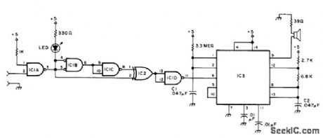
Indication of static state of terminal in digital logic is made audible forblind experimenter by using NE556 timer IC3 as oscillator controlled by IC1 (SN74132N) and lC2 (SN7486N). Any logic transition from 1 to 0 or 0 to 1, lasting at least 50 ns, is detected and indicated by audio beep. Visual indication is provided by LED that comes on when input is logic 1.-T. Lincoln, A Logic Probe You Can Hear, 73Magazine, Aug. 1976, p 106. (View)
View full Circuit Diagram | Comments | Reading(636)
DIFFERENTIAL_VOLTMETER
Published:2009/7/24 1:34:00 Author:Jessie
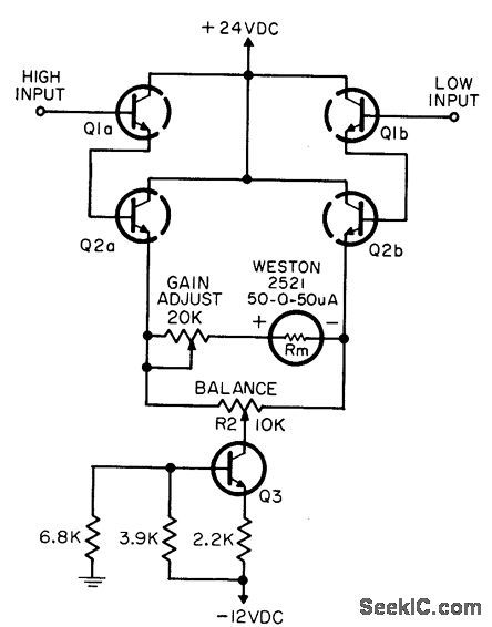
High-impedance differential-input transistorized panel voltmeter has stable zero point, eliminating need for undesirable zero control. Meter com pares voltage under test with known zener regulated reference voltage. Circuit is differential Darlington connected emitter-follower using pair of 2N2060's. Bias point is stabilized by constant-current sync connected to 2N1613 transistor. Accuracy is 1% if unmatched source impedance is less then 10K.-A High-Stability Differential Voltmeter, Electronic Circuit Design Handbook, Mactier Pub, Corp., N.Y., 1965, p 152. (View)
View full Circuit Diagram | Comments | Reading(1426)
TUNER_USES_IC
Published:2009/7/2 22:37:00 Author:May

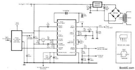

Availability of Signetics NE563 IC having about 180 transistors greatly simplifies construction of high-qualitiy FM tuner . IC includes circuits for converting IF output signal to lower frequency for driving phaselocked loop of demodulator . use of varicap front end permits switched or continuous Tuning with 100K Helipot or with switched preset 100k pots connected between +12 V and ground .tuning contorls can be remotely located .After 60 dB of amplification in NE563 IC,signal passes through ceramic filter F(Vernitron FM-4 or Toko CFS) before being fed back through C5 to IC for mixing with crystal -controlled 9.8-MHz local oscillator.Article covers construction and operation of tunner in detail.-J.B.Dance,High-Quanlity F.M.Tuner,Wireless World ,March 1975,p 111-113. (View)
View full Circuit Diagram | Comments | Reading(2194)
LISTEN_TO_LOGIC
Published:2009/7/2 22:34:00 Author:May


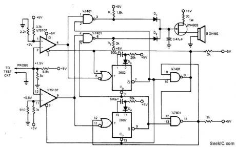
Gives audio indication of TTL states when probe is held on IC pin. Input level above 2 V makes 2N48O3 UJT oscillate at about 400 Hz and give tone from loudspeaker.Logic 0 at probe input gives lower frequency.Logic pulse transitions trigger 2602 dual monos for 1 s, modulating tones at about 1-s rate.Monos also drive two-gate latch that prevents either mono from firing two consecutive times.-I. Simon, Audio Output Eases Logic Level Checking, EDNMagazine, June 20, 1975, p 116and 118. (View)
View full Circuit Diagram | Comments | Reading(775)
1_kHz_BANDPASS_2
Published:2009/7/2 22:30:00 Author:May
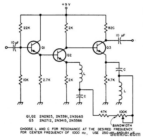
Three-stage audio filteruses two series resonant circuits to give very narrow audio passband Amount of feedback determines Q and bandwidth.-Circuits,Magazine, March 1974, p 89. (View)
View full Circuit Diagram | Comments | Reading(540)
CMOS_LOGIC_PROBE
Published:2009/7/2 22:29:00 Author:May

Designed for wiring into microprocessor to show status of an important terminal, as troubleshooting aid. LEVEL LED is on for TTL input of 1 and off for input of 0. EDGE LED lights momentarily when input changes from 1 to 0 or 0 to 1. Use of CMOS inverting buffer 3a at input prevents probe from affecting microprocessor.-F. A. Weissig, A CMOS Logic Probe, BYTE, Oct. 1977, p 11. (View)
View full Circuit Diagram | Comments | Reading(2110)
DUAL_RANGE_D_C_VOLTMETER
Published:2009/7/24 1:33:00 Author:Jessie

With switch in position 2, serves as standard 0-50 v d-c voltmeter. With switch in position 1, R1 is shunted across 50-my, 1-mc meter to allow about 3 ma through 27+, 1-w tenor diode CR1-CR2 diode 1N540 is for temperature compensation. About 27 v is then held across the diodes, and meter scale represents 27 to 32 v, with sensitivity of 0.1 v d-c per division. R3 is used for calibration.-M. W. Raybin, Dual Range DC Voltmeter, EEE, 10:12,p 31. (View)
View full Circuit Diagram | Comments | Reading(609)
8_TRACE_LOGIC_DISPLAY
Published:2009/7/2 22:25:00 Author:May

Adapter for standard oscilloscope shows time relationship between pulses at eight different locations in digital circuit, for troubleshooting and isolation of glitches. Almost any general-purpose CRO can be used, but triggered sweep improves usefulness. Multiplexer feeds each input in turn to Y input of CRO, under control of counter. Article covers operation and use of adapter.-R. A.Johnson, Eight Trace Scope Adapter, 73 Magazine, Sept. 1976, p 108-110. (View)
View full Circuit Diagram | Comments | Reading(1266)
LED_DISPLAY_FOR_TTL
Published:2009/7/2 22:22:00 Author:May

Useful for observing TTL levels when CRO is not available. A1 and A2 are 74123 dual retriggerable mono MVBRs with clear, used to tum on LEDs when input transitions are detected. Even very short pulses are made visible because mono stretches pulse length. Table shows how LED indications are interpreted.-B. Voight, The TTL One Shot, 73 Magazine, Feb,1977, p 56-58. (View)
View full Circuit Diagram | Comments | Reading(2597)
FASTER_SLEWING
Published:2009/7/2 22:18:00 Author:May

Single transistor stage at output of opamp increases slewing rate by factor equal to gain of transistor stage. Choose R1 to meet output impedance requirements and current rating of supply. R2 is then made equal to R1 divided by desired gain of transistor stage. Collector of Tr1 should be at 0 V when output of opamp is 0 V. assuming feedback loop is not closed by Rf. Article gives design equations.-L. Short. Faster Slewing Rate with 741 Op-Amp. Wireless World. Jan. 1973. p 31 (View)
View full Circuit Diagram | Comments | Reading(545)
PROBE
Published:2009/7/2 22:17:00 Author:May
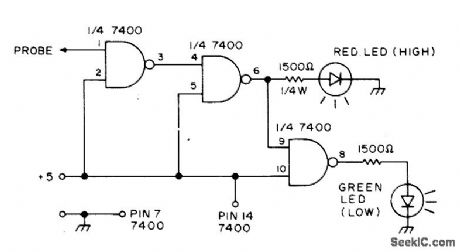
Red LED comes on to indicate thattest point is at high logic level, while green LED signifies low level. Circuit uses one 7400 quad dualinput NAND gate.-S. Uhrig, Check Logic with This Simple Probe, 73 fidagazine, Dee. 1974, p 76. (View)
View full Circuit Diagram | Comments | Reading(1921)
RED_GREEN_LEVEL_DISPLAY
Published:2009/7/2 22:14:00 Author:May

Level detector can be used with TTL, DTL, and RTL, as probe for troubleshooting. Indicator is Monsanto MV5491 dual red/green LED, with 220 ohms in upper lead to +5 V supply and 100 ohms in lower +5V lead because red and green LEDs in parallel back-to-back have different voltage re quirements. Will furnish green indication on high or plus signal and red indication on low or false signal. Supply voltage of +5 V can be taken from equipment under test. Circuit requires SN75451 driver ICs and two sections of SN7404 hex invelter.-K. Powell, Novel Indicator Circult, Ham Radio, April 1977, p 60-63. (View)
View full Circuit Diagram | Comments | Reading(729)
RECTIFIER_WITHOUT_DC_OFFSET
Published:2009/7/2 22:11:00 Author:May
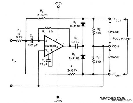
Avoids drawback ofJarge nonlinearity at low signal levels. by isolating AC of opamp from DC output.Circuit has wide bandwidth, as required for rectifying 20-kHz input signal with high precision, Output coupling capacitor C3 is low-Ieakage Mylar; for low-frequency operation. it can be replaced with two back-to-back low-leakage tantalums. D1 and D2 should be matched for forward voltage at peak load current. Use Hewlett-Packard 5082-2810 hot-carrier diodes instead to improve operation at millivolt signal levels or at higher frequencies.-D. Belanger. Single Op Amp Full-Wave Rectifier Has No DC Offset. EDN Magazine. April 5. 1977. p 144 and 146. (View)
View full Circuit Diagram | Comments | Reading(839)
AUDIBLE_LOGIC_INDICATOR
Published:2009/7/2 22:10:00 Author:May
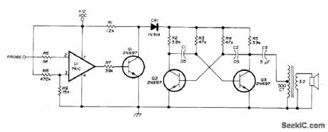
Audio oscillator Q1-Q2-Q3 is isolated from TTL by opamp U1 wired as Schmitt trigger. Opamp acts as highinput-impedance inverter. Reference level is set at +1.6 V by R8-R9 for TTL-compatible logic (about midway between high and low logic levels). When probe input is below +1.6 V, opamp output of about 10.5 V saturates Q1and disables Q2-Q3 to cut off tone. When probe voltage is above +1.6 V, U1 output is about 2 V which cuts off Q1 and allows Q2-Q3 to generate tone indicating high logic.-H. F. Batie, Versatile Audio Oscillator, Ham Radio, Jan. 1976, p 72-74. (View)
View full Circuit Diagram | Comments | Reading(657)
| Pages:1130/2234 At 2011211122112311241125112611271128112911301131113211331134113511361137113811391140Under 20 |
Circuit Categories
power supply circuit
Amplifier Circuit
Basic Circuit
LED and Light Circuit
Sensor Circuit
Signal Processing
Electrical Equipment Circuit
Control Circuit
Remote Control Circuit
A/D-D/A Converter Circuit
Audio Circuit
Measuring and Test Circuit
Communication Circuit
Computer-Related Circuit
555 Circuit
Automotive Circuit
Repairing Circuit