
Circuit Diagram
Index 1132
Ultra_low_noise_preamplifier
Published:2009/7/24 0:18:00 Author:Jessie


The SL561 used in this circuit is a high-gain low-noise preamplifier designed for audio/video applications at frequencies up to 6 MHz. Figure 2-6B shows gain versus frequency for various values of C1, and Fig. 2-6C shows gain versus various values of RSET. Figure 2-6D shows the electrical characteristics. Figure 2-6E shows harmonic distortion. (View)
View full Circuit Diagram | Comments | Reading(742)
Two_stage_wideband_arnphfier
Published:2009/7/24 0:16:00 Author:Jessie

This circuit uses two SL550s (Fig. 2-4), with the first stage connected as a common emitter, and the second stage common base. Stable gains of up to 65 dB can be achieved by the proper selection of R1/R2. The bandwidth is 5 to 103 MHz, with a noise figure slightly greater than 2.0 dB. (View)
View full Circuit Diagram | Comments | Reading(718)
Single_chip_low_noise_wideband_amplifier_with_external_gain_AGC
Published:2009/7/24 0:15:00 Author:Jessie


The SL550 used in this circuit is a general-purpose wideband linear amplifier with remote gain/AGC control. Figure 2-4B shows the electrical charac-teristics. Figure 2-4C shows frequency response. The input capacitance (typically 12 pF at 60 MHz) is independent of frequency. The input resistance (about 1.5 kΩ at 10 MHz) decreases with frequency and is typically 500Ω at 60 MHz. Typical gain/ACC voltage is 0.6 V (Ic=1μA) to 0.8 v (IC= 2 mA) applied to pins 2 and 3 (Fig. 2-4D). If full output swing is not required, omit R1, as shown in Fig. 2-4B.A high-impedance output current can be obtained by taking the output from pin 6 (with pin 7 open circuit). Maximum output current is 2 mA peak, with an output impedance of 350 Ω. Gain variation with temperature can be reached (at the expense of noise figure) by decoupling pin 13 and leaving pin 12 open circuit, as shown in Figs. 2-4E and 2-4F. A low input impedance (25 Ω) can be obtained by decoupling pin 11 and applying the input to pin 12 (with pin 13 open circuit). R2 eliminates high-frequency instability, and it can be omitted of the IC is soldered directly to a PC board. (View)
View full Circuit Diagram | Comments | Reading(524)
ABSOLUTE_VALUE_AMPLIFIER
Published:2009/7/2 21:49:00 Author:May

Generates positive output voltage for either polarity of DC input. Opamp and diode types are not critical. Accuracy is highest for input voltages greater than 1 V. Opamp is noninverting on positive signals and inverting on negative signals.- Signetics Analog Data Manual. Signetics, Sunnyvale. CA. 1977. p 641-643. (View)
View full Circuit Diagram | Comments | Reading(0)
19_kHz_NOTCH
Published:2009/7/2 21:48:00 Author:May
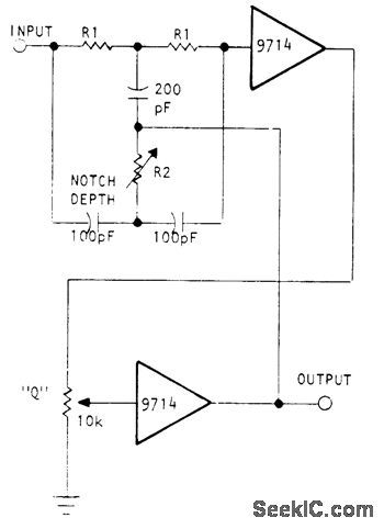
Used in commercial FM transmitters to eliminate 19-kHz program material from stereo encoder. Uses Optical Electronics 9714 opamp in circuit that gives unity passband gain below center frequency, 0.7 gain above center frequency, and Iess than 0.001 gain at notch frequency. Provides adjustments for notch rejection level and Q. R1 is 84K, and R2 is 36K in series with 10K pot.- Precision Notch Filter, Optical Electronics, Tucson, AZ, Application Tip 10255. (View)
View full Circuit Diagram | Comments | Reading(649)
1_kHz_CASCADED_OPAMP_BANDPASS
Published:2009/7/2 21:47:00 Author:May
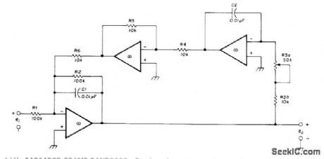
Bandwidth of only 71 Hz is achieved by using four identical three-opamp filters in series, for increased selectivity in communication or RTTY receiver. Values for R1 and R2 are made variable for first filter stage, but pot is used for R3 in all four stages so they can betuned to same center frequency. Batteries are used for supply, asfilter draws only 17 mA.-F. M. Griffee, RC Active Filters Using Op Amps, Ham Radio, Oct. 1976, p 54-58. (View)
View full Circuit Diagram | Comments | Reading(442)
RTL_TTL_PROBE
Published:2009/7/2 21:46:00 Author:May
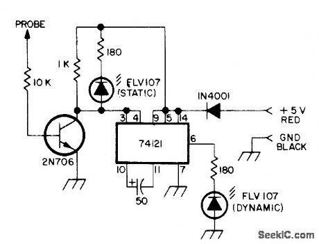
Static LED indicates logic Ievel at probe tip. Dynamic LED indicates presence of high or 1 pulse at probe tip even though momentary, because circuit stretches pulse to about 50 μs for easy visibility. Pulse stretcher requires at least 100-ns 4-V pulse. 1N4001 diode protects against reversed power leads. Probe requires +5 V from circuit under test. LEDs and transistor are not criticaL-Circuits, 73 Magazine, April 1974, p 31. (View)
View full Circuit Diagram | Comments | Reading(620)
Lozu_dropout_P_channel_linear_regulator
Published:2009/7/24 1:30:00 Author:Jessie

Figure 7-33 show a MAX684 linear regulator. The output voltages are: MAX682 3.3 V, MAX683 5.0 V, MAX684 3.3 V, and MAX685 3.0 V. The supply range is 2.7 V to 11.5 V, the maximum dropout is 300 mV at 200 mA output, the maximum quiescent current is 15 μA, the shutdown current is 1 μA (maximum). MAXIM NEW RELEASES DATA BOOK. 1994. P. 4-49.
(View)
View full Circuit Diagram | Comments | Reading(487)
3_W_POWER_AMPLIFIER_FOR_SPLIT_PHASE_MOTOR
Published:2009/7/24 1:29:00 Author:Jessie
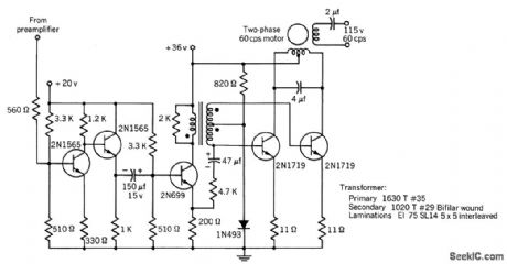
Capacitor tunes motor to make load more resistive. Feedback is used to lower output impedance and thereby improve transient response of motor. Used in digital servo system.-Texas Instruments Inc., Transistor Circuit Design, McGraw-Hill, N.Y., 1963, p 493. (View)
View full Circuit Diagram | Comments | Reading(591)
HALF_WAVE_RECTIFIER
Published:2009/7/2 21:43:00 Author:May

Provides accurate half-wave rectification of incoming signal. Gain is 0 for positive signals and -1 for negative signals. Diodetypes are not critical. Polarity can be inverted by reversing both diodes. With opamp shown, circuit will function up to 10 kHz with less than 5% distortion.- Sig netics Analog Data Manual. Signetics. Sunnyvale. CA. 1977. p 641-643. (View)
View full Circuit Diagram | Comments | Reading(2939)
LOGIC_STATE_PROBE
Published:2009/7/2 21:41:00 Author:May
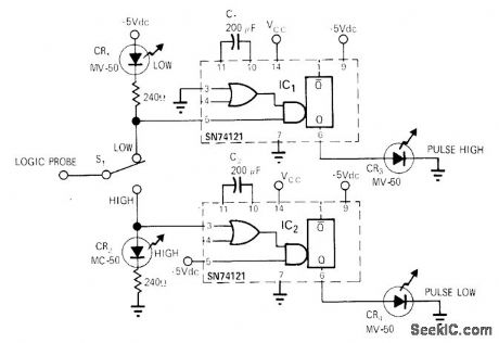
Useful for low-repetition-rate applications having single narrow pulses, as in computer interfaces and logic control systems. Pulses as narrow as 50 ns are stretched by mono so they provide LED indication. If teady state of circuit under test is low, CR1 will light when S1 is in in low position. If steady state is high, CR2 will light when switch is high. Other two lamps indicate presence of pulse superimposed on steady-state signal. If repetition frequency of pulse is high, pulse light Speed Logic Probe, EDNlEEEMagazine, Nov. 1,1971, p 51. (View)
View full Circuit Diagram | Comments | Reading(815)
FET_PNP_D_C_MILLIVOLTMETER
Published:2009/7/24 1:29:00 Author:Jessie

Differential amplifier uses pair of simple feedback amplifiers having voltage gain of 3, output impedance of 50K, input sensitivity of 20. meg/v, and common mode rejection ratio of 1,000 to 1.-Texas Instruments Inc., Solid-State Communications, McGraw-Hill, N.Y., 1966, p 136. (View)
View full Circuit Diagram | Comments | Reading(638)
TRIAGLE_AND_SQUARE_WAVEFORM_GENERATOR
Published:2009/7/2 21:39:00 Author:May
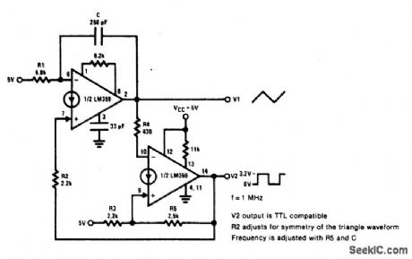
View full Circuit Diagram | Comments | Reading(489)
COMPLETE_3_W_400_CPS_SERVO_AMPLIFIER
Published:2009/7/24 1:28:00 Author:Jessie

Is capable of driving 3.w servo motor in ambient of -55 to 125℃, if capacitors for 125℃ are used. Gain can be adjusted over range of 20,000 to 80,000 amp per amp by adjusting RF in driver circuit. Gain varies less thon 10% over operating temperature range.- Transistor Manual, Seventh Edition, General Electric Co., 1964, p 225. (View)
View full Circuit Diagram | Comments | Reading(626)
Charge_pump_voltage_converter
Published:2009/7/24 1:28:00 Author:Jessie

Figure 7-32 shows a MAX619 connected to provide a 5-V, 15-mA output, with 2-V to 3.6-V input, using two inexpensive capacitors, The quiescent current is 150 μA (max) with 10μA (max) shutdown current. MAXIM NEw RELEAsEs DATA BOOK, 1994, P. 4-37.
(View)
View full Circuit Diagram | Comments | Reading(615)
SIGNAL_SEPARATOR
Published:2009/7/2 21:37:00 Author:May

Circuit shown for Harris HA-2530 opamp separates input voltage into its positive and negative components. Diodes steer components to separate outputs. Appli-cations include feeding outputs into differential amplifier to produce absolute-value circuit for multiplying or averaging functions. For bandwidth of 1 MHz. dynamic range is 100 mV to 10 V peak.- Linear & Data Acquisition Products.}| Harris Semiconductor. Melbourne. FL. Vol. 1. 1977. p 7-54-7-55 (Application Note 516). (View)
View full Circuit Diagram | Comments | Reading(667)
PREFERRED_PHASE_SENSITIVE_NULL_DETECTOR
Published:2009/7/24 1:26:00 Author:Jessie

Operates d-c relay when sum of input cur rents is zero. Circuit can be adjusted for any operating frequency from 300 to 1,000 cps by selection of C5 and C7; values given are for 500 cps. Consists of ac amplifier, phase-sensitive detector, and relay control tube.-NBS, Handbook Preferred Circuits Navy Aeronautical Electronic Equipment, Vol. 1, Electron Tube Circuits, 1963, PC 78, p 78-2. (View)
View full Circuit Diagram | Comments | Reading(667)
High_speed6_A_single_MOSFET_drivers
Published:2009/7/24 1:26:00 Author:Jessie
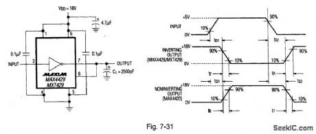
Figure 7-30 shows the MAX4429/MXT429 connected to translate TTL/CMOSinputs to high-voltage/high-current outputs,The output impedance is 1.5 Ω witha 6-A current.Delay time is 40 ns, with 25-ns rise/fall times(into a 2500-pF load).Figure 7-31 shows the timing test circuit.The supply range is 4.5 V to 18 V,with anoutput swing to within 25 mV of VDD and ground.MAXIM NEW RELEASES DATABook,1994, P.4-31.4-35, (View)
View full Circuit Diagram | Comments | Reading(659)
4_W_SERVO_MOTOR_DRIVE
Published:2009/7/24 1:25:00 Author:Jessie

Emitter-follower (common collector) push-pull amplifier gives stable output stage gain along with low-impedance drive for 1 to 4-w servo motors. Forward bias of 1.4 v is developed across D1 and D2, while D3 and D4 protect transistors from inductive load generated voltages that exceed emitter. base breakdown. Efficiency is better thon 60%.- Transistor Manual, Seventh Edition, General Electric Co., 1964, p 223. (View)
View full Circuit Diagram | Comments | Reading(675)
Ratio_V_F_converter
Published:2009/7/24 1:14:00 Author:Jessie

Fig. 12-25 This circuit converts the ratio of two voltages to an equivalent frequency (essentially the same function as performed by the circuit of Fig. 12-16). In this circuit, the two op amps convert the inputs to proportional currents. The 1-kΩ scale-factor trim is adjusted so that the frequency output equals the ratio of V1/V2 x 10 kHz. Full-scale output is 15 kHz. The circuit can accept positive inputs when the op-amps are rearranged, as shown in Figs. 12-25B or 12-25C. Trimming out the offset in the Op amp gives the ratio converter better linearity and accuracy, e trim circuit Fig. 12-25B needs stable positive and negative supplies for the offset trimmer, but the trim In Fig, -25C needs only an astable positive supply. Unmarked components in Fig. 12-25C are the same as those in Fig. -25B. (View)
View full Circuit Diagram | Comments | Reading(661)
| Pages:1132/2234 At 2011211122112311241125112611271128112911301131113211331134113511361137113811391140Under 20 |
Circuit Categories
power supply circuit
Amplifier Circuit
Basic Circuit
LED and Light Circuit
Sensor Circuit
Signal Processing
Electrical Equipment Circuit
Control Circuit
Remote Control Circuit
A/D-D/A Converter Circuit
Audio Circuit
Measuring and Test Circuit
Communication Circuit
Computer-Related Circuit
555 Circuit
Automotive Circuit
Repairing Circuit