
Circuit Diagram
Index 1129
Micropower_V_F_converter_10_kHz
Published:2009/7/24 1:43:00 Author:Jessie

Fig. 12-29 In this circuit, a 0- to 5-V input produces a 0 to 10-kHz output with a linearity of 0.02%. Drift is about 40 ppm/℃. Maximum current consumption is about 135μA-far below most IC V/F converters. To trim, apply 50 mV and select a value (typical 21 kΩ) at the C1 input for a 100-Hz output. Then, apply 5 V and adjust the 50-kΩ trim for a 10-kHz output. Linear Technology Linear Applications Handbook 1990 p AN23-11. (View)
View full Circuit Diagram | Comments | Reading(570)
1_kHz_BIQUAD_BANDPASS
Published:2009/7/2 23:18:00 Author:May

Three 741 opamps are connected to give two integrators and inverter. Overall gain is -Q, determined by value of input resistor used. Circuit is tuned by varying capacitors in steps. Absolute bandwidth remains constant asfrequency changes. Chief applications are in telephone systems, where identical absolute-bandwidth channels are required.-D. Lancaster, Active-Filter Cookbook, Howard W. Sams, Indianapolis, IN, 1975, p 159-164. (View)
View full Circuit Diagram | Comments | Reading(757)
UNITY_GAIN_FEED_FORWARD
Published:2009/7/2 23:17:00 Author:May

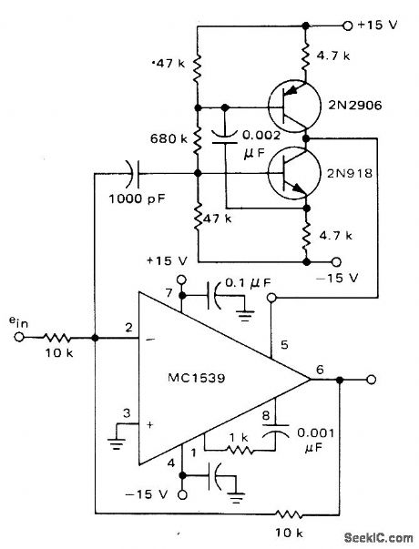
Provides 10 V P-P output signal at 2 MHz when gain of feedforward amplifier is increased to give closedloop gain of 10. Provides fast response to stepfunction input. with slow settling. High-frequency circuit takes over completely when input frequency is too high for input stage to respond.-E. Renschler. The MC1539 Operational Amplifier and Its Applications. Motorola. Phoenix. AZ. 1974. AN-439. p 20. (View)
View full Circuit Diagram | Comments | Reading(658)
1_kHz_THIRD_ORDER_LOW_PASS
Published:2009/7/2 23:17:00 Author:May

Circuit using 741 or equivalent opamp consists of unity-gain first-order section followed by equal-component voltage-controlled voltage-source secondorder section.-H. M. Berlin, Design of Active Filters, with Experiments, Howard W. Sams, Indianapolis, IN, 1977, p 113-114. (View)
View full Circuit Diagram | Comments | Reading(800)
VOLTAGE_TUNED_STATE_VARIABLE
Published:2009/7/2 23:16:00 Author:May


Provides choice of high-pass, bandpass, and low-pass outputs, each with cutoff frequency variable between 1 and 6 kHz by varying control voltage between -10 V and +15 V,Output load resistor sets voltage gain between input and output. Gain-control input varies gain from maximum set by load resistor down to zero.Input signals must be limited to 100 mV because input circuit is differential amplifier operating without feedback.-D. Lancaster, Active-Filter Cookbook, Howard W. Sams, Indianapolis, IN, 1975, p 203-205. (View)
View full Circuit Diagram | Comments | Reading(749)
320_Hz_LOW_PASS
Published:2009/7/2 23:14:00 Author:May

Frequency dependent negative-resistance circuit uses 747 dual opamp, Signal source used as input should have low resistance, and load should have high resistance. Voltage-follower stages can be used to isolate both input and output of filter.-R.Melen and H. Garland, Understanding IC Operational Amplifiers, Howard W. Sams, Indianapolis, IN, 2nd Ed.,1978, p 104-105. (View)
View full Circuit Diagram | Comments | Reading(592)
2_W_2_METER_PHASE_LOCKED_FM_TRANSMIT_TER
Published:2009/7/2 23:13:00 Author:May
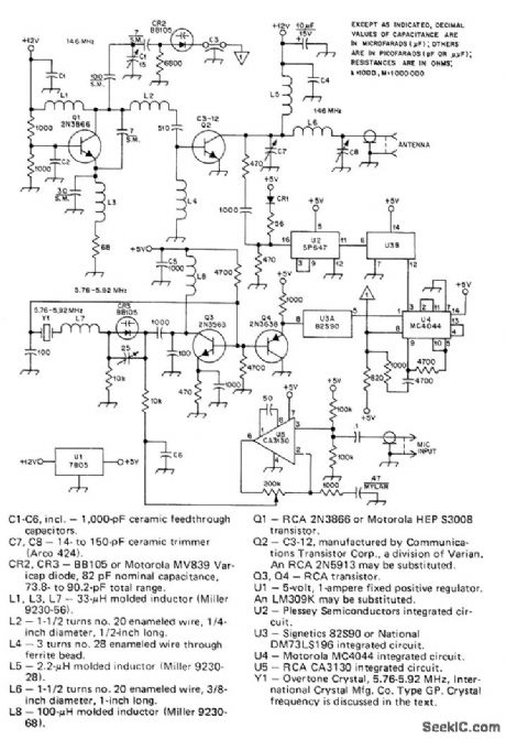
Operating frequency of 144-148 MHz is generated directly, without using frequencymultiplier stages. Oscillator stability is achieved by phase-Iocking oscillator to crystal. Tuning range of 143-149 MHz corresponds to varactor control voltage of 1-4 V, which maintains proper loop gain across entire band, ECL decade divider U2 is Plessey SP647 driving Schottkyclamped divider U3B to give overall division of 50. Phase detector and Ioop amplifier functions are in U4. Pierce crystal oscillator Q3 feeds buffer Q4 interface with TTL levels. Microphone preamp U5 is slightly overdriven so speech waveform is clipped or Iimited. With phaseIocked circuit, frequency stability is as good as that of crystal used in reference oscillator. Divide desired operating frequency by 25 to get crystal frequency.-A. D. Helfrick, A Phase-Locked 2-Meter FM Transmitter, QST, March 1977, p 37-39, (View)
View full Circuit Diagram | Comments | Reading(873)
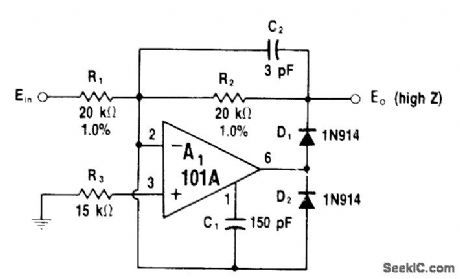
FET_D_C_MILLIVOLTMETER
Published:2009/7/24 1:42:00 Author:Jessie

Uses differential amplifier assembled from pair of simple two stage feedback amplifiers having voltage gain of 3. Input sensitivity of meter is 20 meg per v and common mode rejection ratio is 1,000 to 1. Temperature characteristics are reasonably good when using matched let's.-Texas Instruments Inc., Transistor Circuit Design, McGraw-Hill, N.Y., 1963, p 522. (View)
View full Circuit Diagram | Comments | Reading(810)
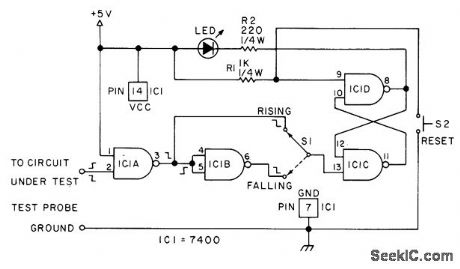
LATCHING_PROBE
Published:2009/7/2 23:12:00 Author:May
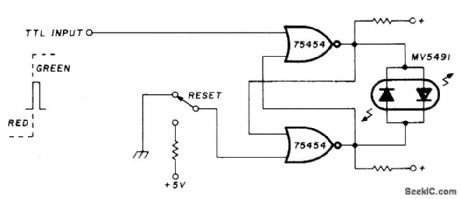
TTL pulse catcher can be used as logic probe for IC troubleshooting. Uses Monsanto MV5491 dual red/green LED, with 220 ohms in upper lead to +5 V supply and 100 ohms in lower +5 V lead because red and green LEDs in parallel back-to-back have different voltage requirements. SN75454 driver circuit is cross-coupled to form latch or memory element. Positive-going pulse sets latch and makes LED change color to indicate arrival of pulse. Latch must be reset manually with RESET switch. Also useful for locating intermittents such as glitches; probe can be left connected to circuit under test, to see if latch hasbeen set by unwanted signaL-K. Powell, Novel Indicator Circuit, Ham Radio, April 1977, p 60-63. (View)
View full Circuit Diagram | Comments | Reading(730)
MICROMODULE_FOR_16_MC_CLOCK_RAIE
Published:2009/7/24 1:42:00 Author:Jessie

Flip-lop arrangement of two standard gales, with capacitor-resistor-diode gates fled to bases for trigger input, operates under worstcase temperature conditions with two standard gate loads.-A. S. Rettig, Computers in the Front Lines: Micromodules Make it Possible, Electronics, 36:1, p 77-81. (View)
View full Circuit Diagram | Comments | Reading(557)
TEST_PROBE
Published:2009/7/2 23:06:00 Author:May
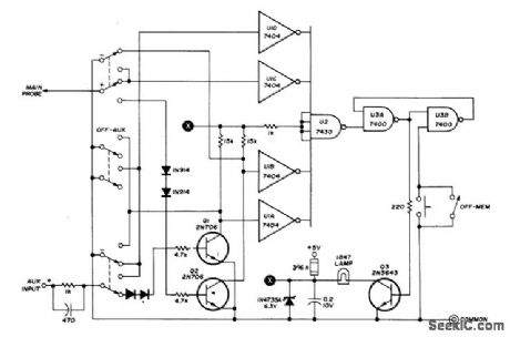
Checks binary levels and pulse coincidence. Indicator lamp, driven by switching transistor 03, is bright enough to be seen in sunlight. Close OFF-MEM switch when using probe as binary level indicator, to eliminate need for pushing button continuously. At AUX position of main switch, two inputs are needed at same time. To check for coincidence, connect patch cord from AUX jackto second point being checked in logic circuit. All signal diodes are 1N914. Probe drain is about 160 mA; changing to LED would cut drain to 6O mA.-R. H. Fransen, Improved Logic Test Probe, Ham Radio, Dec. 1973, p 53-55. (View)
View full Circuit Diagram | Comments | Reading(615)
Ultraprecision_V_F_converter
Published:2009/7/24 1:42:00 Author:Jessie

Fig. 12-28 This circuit is capable of better than 0.2% error and 0.003% nonlinearity for a ±20℃ range about room temperature. The basic V/F function of the LM331 is augmented by an LM308A connected as an integrator. To trim, connect the input to ground, and set the offset adjustment for zero output. Remove the ground and apply -10.000 V to the input and adjust the 5-kΩ scale factor trim for 10-kHz output. National Semiconductor Linear Applications Handbook, 1991 p. 1310. (View)
View full Circuit Diagram | Comments | Reading(1347)
AUDIBLE_PROBE
Published:2009/7/2 23:00:00 Author:May
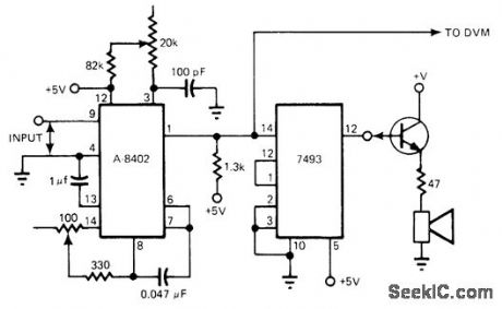
Speeds troubleshooting by eliminating need to look at meter, and prevents possible damage to logic under test by minimizing possibility of shorts occurring if probe slips when looking at meter. Components used with A-8402 IC give 1-kHz output for 6-V input.Binary counter divides this signal to give output in low audio range and converts to square wave more suitable for driving loudspeaker. Probe can also serve as input for digital voltmeter.When probing TTL circuits, probe gives low frequency for 0 state, high frequency for 1, and middle frequency for open circuit. Output transistor type is not criticaL-G. E, Row, Audible Logic Probe Doubles as DVM Input Section, EDNMagazine, Oct. 20, 1977, p 82. (View)
View full Circuit Diagram | Comments | Reading(497)
SINGLE_LED_TUNING_INDICATOR
Published:2009/7/2 22:58:00 Author:May
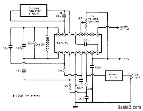
Circuit shown, when driven by IF output of FM tuner, permits tuning for maximum brightness of single LED such as 50824403. Article gives choice of two tuning indicator circuit awangements that can be used with the SBA750 limiting IF amplifier and detector IC. Recommended version of tuning indicator uses Plessey SL3046 five-transistor array with discrete resistors and capacitor to drive LED. Arrangement gives very clear, sensitive indication of correct tuning point to within a few millivolts.-J. A. Skingley, Sensitive F.M. Tuning Indicator, Wireless World, June 1974, p 173-174. (View)
View full Circuit Diagram | Comments | Reading(1332)
PREFERRED_AMPLIFICATION_1200_PREAM_PLIFIER
Published:2009/7/24 1:39:00 Author:Jessie

Used with instrument servo motor controller to increase available gain. Chopper is used with d-c outputs only.-NBS, Handbook Preferred Circuits Navy Aero. nautical Electronic Equipment, Vol. I, Electron Tube Circuits, 1963, PC 74, p 74-2. (View)
View full Circuit Diagram | Comments | Reading(594)
_5_V_adjustable_inverting_PWM_regulators
Published:2009/7/24 1:37:00 Author:Jessie


Figure 7-34 shows a MAX735 connected in a basic circuit to provide a 200-mA, -5-V output with a +4.0-V to +6.2-V input. Figure 7-35 shows the corresponding circuit using surface-mount components. Figure 7-36 shows the circuit using through-hole components (at commercial temperature ranges). Figure 7-37 shows the circuit using through-hole components (for all temperature ranges). Figure 7-38 shows component suppliers and Fig. 7-39 shows the block diagram with typical external components. The MAX755 operates from a +2.7-V to +9-V input and generates an adjustable negative output, depending qn the values of R3 and R4. The relationship is:Resistor R3 can be any value from 10 kΩ to 20 kΩ, VOUT is limited to 11.7 V -VIN. The quiescent current is 1.6 mA, with a 10-μA shutdown current. MAXIM NEW RELEASES DATA Book, 1994, P. 4-111, 4-115, 4-116, 4-117. (View)
View full Circuit Diagram | Comments | Reading(881)
400_CPS_PREAMP_FOR_TWO_PHASE_SERVO_MOTOR
Published:2009/7/24 1:35:00 Author:Jessie

Bias point and gain are stable over wide temperature range, from -55 to 125℃.No selection of transistors is required. Bias design procedure and design equations are given.- Transistor Manual, Seventh Edition, General Electric Co., 1964, p 218. (View)
View full Circuit Diagram | Comments | Reading(581)
HIGH_SPEED_HALF_WAVE_RECTIFIER
Published:2009/7/2 22:57:00 Author:May

Produces inverted haff-wave replica of input signal with Iow error at frequencies up to 100 kHz. C1 provides feed-forward compensation. For negative-going output. reverse connections to diodes.-W. G. Jung. IC Op-Amp Cookbook. Howard W. Sams. Indianapolis. IN. 1974. p 191-192 (View)
View full Circuit Diagram | Comments | Reading(690)
FAST_TTL_PROBE
Published:2009/7/2 22:56:00 Author:May
RS flip-flop wired from NAND gate detects pulses as short as combined gate delays of NAND sections forming flip-flop (about 30 ns). Circuit changes state at start of pulse, with LED monitoring flip-flop output.After pulse has been detected, circuit must be reset with S2. Will work with either positive-or negative-going pulse, as selected by S1.-W. A.Walde, Build a TTL Pulse Catcher, BYTE, Feb.1976, p 58 and 60. (View)
View full Circuit Diagram | Comments | Reading(955)
FM_MODULATOR_
Published:2009/7/2 22:53:00 Author:May
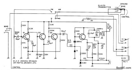
Developed to permit FM operation on AM transceiver. Consists of microphone preamplifier, driver amplifier, and 8-MHz crystal oscillator providing 24-MHz output.Audio from modulator drives variable-capacitance diode D1 (which can be silicon switching diode) in oscillator circuit. Adapter feeds AM transmitter in which frequency multipliers inGrease deviation to about 8.5 kHz,To reduce deviation for narrow-band FM,adjust 500K pot in preamρ.-R .Orozco,Jr.,Put That AM Rig on FM,73 Maga,April 1976,p 34-35. (View)
View full Circuit Diagram | Comments | Reading(904)
| Pages:1129/2234 At 2011211122112311241125112611271128112911301131113211331134113511361137113811391140Under 20 |
Circuit Categories
power supply circuit
Amplifier Circuit
Basic Circuit
LED and Light Circuit
Sensor Circuit
Signal Processing
Electrical Equipment Circuit
Control Circuit
Remote Control Circuit
A/D-D/A Converter Circuit
Audio Circuit
Measuring and Test Circuit
Communication Circuit
Computer-Related Circuit
555 Circuit
Automotive Circuit
Repairing Circuit