
Circuit Diagram
Index 1135
600_Hz_NOTCH
Published:2009/7/2 21:10:00 Author:May
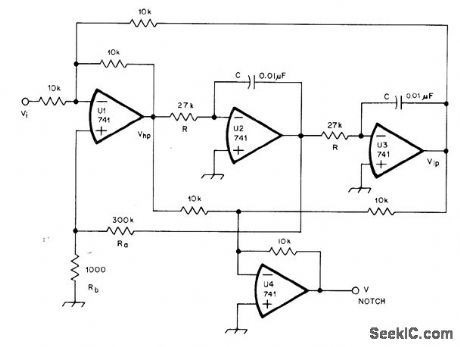
With values obtained from design equations and graph in article, state-variable or universal filter provides a of 100 with four opamps. Notch filter is achieved by adding low-pass and high-pass outputs equally, for feed to dual-input summing amplifier.M.Berlin, The State-Variable Filter,QST, April 1978, p 14-16. (View)
View full Circuit Diagram | Comments | Reading(1082)
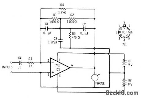
AC_MILLIVOLTMETER
Published:2009/7/2 21:10:00 Author:May

View full Circuit Diagram | Comments | Reading(0)
14_kHz_TWIN_T_BANDPASS
Published:2009/7/2 21:08:00 Author:May

Combination of passive twin-T bandpass filter and 741 opamp gives simple audio filter for amplifying narrow frequency band (about 300 Hz wide) centered on 1.4 kHz. Filter ean be tuned to other frequencies by replacing R1 and R2 with 10K pots. Frequency is equal to 1/6.28RC where R is value in ohms of R1 and R2 and C is capadtance in farads of C1 and C2. R3 is half of R1.-F. M. Mims, Integrated Circuit Projects, Vol. 2, Radio Shack, Fort Worth, TX, 1977, 2nd Ed., p 71-80.
(View)
View full Circuit Diagram | Comments | Reading(1165)
AMPLIFIED_TTL_INTERFACE_FOR_VMOS
Published:2009/7/2 21:08:00 Author:May

Bipolar voltage amplifier Q1 translates TTL output swing of 0.4 to 2.4 V from 7400 interface to 15V drive signal for S55V01 VMOS peripheral driver. Circuit can be driven by any low-level signal, including ECL, if comparator such as AM686 is used in place of SN7400 quad NAND gate.Switching times of circuit are less than 40 ns in both directions.-L. Shaeffer, VMOS Peripheral Drivers Solve High Power Load Interface Problems, ComputerDesign, Doc. 1977, p 90, 94, and 96-98. (View)
View full Circuit Diagram | Comments | Reading(523)
SUPPRESSED_ZERO_METER
Published:2009/7/2 21:08:00 Author:May

A zener diode placed in series with a voltmeter will prevent the meter from reading until the applied voltage exceeds the zener voltage. Thus, a 10 volt zener in series with a 5-volt meter will allow the condition of a 12 V car battery to be monitored with much greater sensitivity than would be possible with a meter reading 0-15 volts. (View)
View full Circuit Diagram | Comments | Reading(1083)
AF_NOTCH
Published:2009/7/2 21:07:00 Author:May
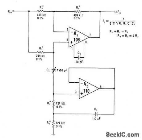
Notch frequency is easily tuned at frequencies below 1 kHz with single capacitor C1 or by replacing R1 and R2 with 249K pot. For higher frequencies, use 118 opamp for A1 and 5K for R3 while lowering other resistances in proportion to R3.Indicated resistance tolerances are necessary for optimum notch depth.-W. G. Jung, IC Op-Amp Cookbook, Howard W.Sams,Indianapolis, IN, 1974, p 340-341. (View)
View full Circuit Diagram | Comments | Reading(575)
WIDE_BAND_AC_VOLTMETER
Published:2009/7/2 21:05:00 Author:May

This voltmeter is capable of measuring ac signals as low as 15 mV at frequencies from 100 Hz to 500 kHz. Full scale sensitivity may be changed by altering the values R1 through R6 (R=VIN/100 μA). (View)
View full Circuit Diagram | Comments | Reading(2079)
741_OPAMP
Published:2009/7/2 21:04:00 Author:May

Power supply and null pot connections for TO-5 metal-can packageand 8-lead DIP package are shown. Maximum rated power supply voltages are ±18 V, but lower voltages may be used. 9-V transistor battery is often used for each supply, but higher voltages will permit larger output signal swing. Pin 3 is inverting input, and pin 4 is noninverting input.With values shown, both input terminals see about same resistance. and output offset can be nulled to zero. Gain of circuit is about l00.-C. Hall, Circuit Design with the 741 Op Amp. Ham Radio. April 1976. p 26-29. (View)
View full Circuit Diagram | Comments | Reading(964)
Cold_junction_compensation_for_the_type_J_thermocouple
Published:2009/7/24 2:19:00 Author:Jessie

Fig. 13-14 This circuit uses an LT1025 and an LT1001 to provide a scaled, cold-junction-compensated output. R6 is a typical value and it might require selection to accommodate the R5 trim range. Alternately, R6 can be re-scaled, and R5 enlarged (with some penalty in trim resolution). Linear Technology Linear Applications Handbook 1990 p. AN28-4. (View)
View full Circuit Diagram | Comments | Reading(813)
CMOS_INTERFACE_FOR_VMOS
Published:2009/7/2 21:03:00 Author:May
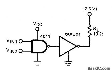
Simple 4011 CMOS gate connection provides required logic interface for S55V01 VMOS that is capable of handling up to 1 A. Switching time is about 25 ns but can be doubled by connecting four CMOS gates in parallel. Vcc can be either 10 or 15V.-L. Shaeffer, VMOS Peripheral Drivers Solve High Power Load Interface Problems, Computer Design, Dee. 1977, p 90, 94, and 96-98. (View)
View full Circuit Diagram | Comments | Reading(454)
175_MHz_40_W_amplifier_136_V_supynly
Published:2009/7/24 2:19:00 Author:Jessie
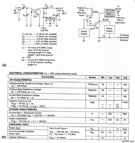
The electrical characteristics for the 2N3924 shown in this circuit are given in Fig.2-14B. (View)
View full Circuit Diagram | Comments | Reading(470)
HIGH_INPUT_IMPEDANCE_MILLIVOLTMETER
Published:2009/7/2 21:01:00 Author:May

View full Circuit Diagram | Comments | Reading(744)
12-V_high-efficiency_controller_boot-strapped
Published:2009/7/24 2:09:00 Author:Jessie


Figure 7-50 shows a MAX1771 connected to provide 12-V output at 0.5 A. vith a 5-V input. Figure 7-51 shows component suppliers. MAXIM NEW RELEASES DATABook. 1995 P.4-20.
(View)
View full Circuit Diagram | Comments | Reading(705)
TOTEM_POLE_ECL_INTERFACE_FOR_VMOS
Published:2009/7/2 21:00:00 Author:May
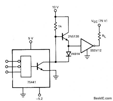
Transistor and diode in totem-pole configuration improve performance of SN75441 ECL-compatible peripheral driver for S55V12 VMOS.-L. Shaeffer, VMOS Peripheral Drivers Solve High Power Load Interface Problems, Computer Design, Dec. 1977, p 90, 94, and 96-98. (View)
View full Circuit Diagram | Comments | Reading(587)
EXTENDED_RANGE_VU_METER_BAR_MODE
Published:2009/7/2 20:58:00 Author:May

View full Circuit Diagram | Comments | Reading(2944)
UNITY_GAIN_AF_CURRENT_AMPLIFIER
Published:2009/7/2 20:57:00 Author:May
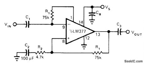
External components are used with National LM377/ 378/379 family of opamps to provide stability at unity gain. Article gives design equations. At frequencies above audio band. gain rises with frequency.to、Mell above 10 at 340 kHz forvalues shown.-D Bohn. AC Unity-Gain Power Buffers Amplify Curren. EDN Magazine. May 5.1977. p113-114. (View)
View full Circuit Diagram | Comments | Reading(555)
TONE_DETECTOR
Published:2009/7/2 20:57:00 Author:May

Output goes low only when input tone has been continuous at desired fre quency for interval exceeding duration of pulse from 555 timer. Circuit can be used to reset an alarm system or to detect TTL level that exceeds predetermined time duration.-Circuits, 73 Magazine, April 1977, p 16a. (View)
View full Circuit Diagram | Comments | Reading(0)
FET_VOLTMETER
Published:2009/7/2 20:56:00 Author:May

This FETVM replaces the function of the VTVM while at the same time ridding the in-strument of the usual line cord. In addition, drift rates are far superior to vacuum tube circuits allowing a 0.5 volt full scale range which is impractical with most vacuum tubes. The low-leakage, low-noise 2N4340 is an ideal device for this application. (View)
View full Circuit Diagram | Comments | Reading(2471)
DVM_AUTO_CALIBRATE_CIRCUIT
Published:2009/7/2 20:54:00 Author:May
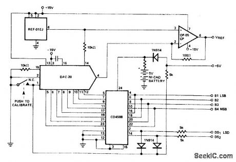
View full Circuit Diagram | Comments | Reading(550)
STORING_SINGLE_PULSE
Published:2009/7/2 20:53:00 Author:May
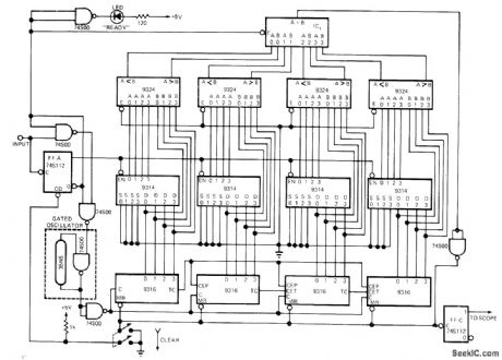
Designed to take single-event positive-going TTL pulse, occurring only once when series of logic conditions is met, and recreating pulse accurately on CRO as square wave in which half of cycle represents original pulse width. FF-A and 9316 binary counters are initially eleared. Input pulse of interest gates delay-line osciliator (lower left) on for duration of pulse width. During this time, binary representation of pulse width is accumulated in 9316 counters, then stored in 9314 D-latches. At same time, final 9324 comparator IC1 is enabled and oscillator is gated on again to reset 9316s and toggle FF-C. Square-wave output of FF-C then represents original pulse width within 35 ns (one clock).-N, L. White, Don't Miss That Single Event Pulse-Store it, EDN Magazine, Sept. 20, 1975, p 70 and 72. (View)
View full Circuit Diagram | Comments | Reading(642)
| Pages:1135/2234 At 2011211122112311241125112611271128112911301131113211331134113511361137113811391140Under 20 |
Circuit Categories
power supply circuit
Amplifier Circuit
Basic Circuit
LED and Light Circuit
Sensor Circuit
Signal Processing
Electrical Equipment Circuit
Control Circuit
Remote Control Circuit
A/D-D/A Converter Circuit
Audio Circuit
Measuring and Test Circuit
Communication Circuit
Computer-Related Circuit
555 Circuit
Automotive Circuit
Repairing Circuit