
Circuit Diagram
Index 1133
TONE_BURST_OSCILLATOR_AND_DECODER
Published:2009/7/2 21:37:00 Author:May

A tone burst sent at the beginning of each transmission is decoded (at receiver) by a PLL causing output from pin 3 of logic gate to turn on carrier-operated switch (COS). (View)
View full Circuit Diagram | Comments | Reading(959)
LOW_COST_HIGH_FREQUENCY_GENERATOR
Published:2009/7/2 21:31:00 Author:May
View full Circuit Diagram | Comments | Reading(552)
STROBE_TONE_BURST_GENERATOR
Published:2009/7/2 21:30:00 Author:May

With a dual supply voltage, the external capacitor on pin 10 can be shorted to ground to halt the 8038 oscillation. The circuit uses a FET switch and diode ANDed with an input strobe signal to allow the output to always start on the same slope. (View)
View full Circuit Diagram | Comments | Reading(0)
100_kHz_QUADRATURE_OSCILLATOR
Published:2009/7/2 21:27:00 Author:May

View full Circuit Diagram | Comments | Reading(662)
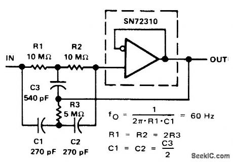
LOW_PASS_WITH_10_kHz_CUTOFF
Published:2009/7/2 21:24:00 Author:May

Simple circult uses only one Texas Instruments SN72310 voitage-fonower opamp,For good temperature stability,use silvered mlca capacitors.- TheLinear and Interface Circuits Data Book for Design Engineers, Texas Instruments,Danas,TX,1973,p 4-39. (View)
View full Circuit Diagram | Comments | Reading(585)
CLOCK_FOR_COMMUTATING_RC_FILTER
Published:2009/7/2 21:22:00 Author:May

Circuit synchronizes multivibrator with line frequency to provide dock waveform required for switching capacitors electronically in npath active filter for rejecting line frequency and harmonics up to fifth. Article gives complete circuit of active filter and describes operation. Clock serves to switch 16 MOSFETs on in turn for commutating 16 capacitors electronically at 16 times line frequency.-K. F. Knott and L. Unsworth, Mains Rejection Tracking Filter, Wireless World, Oct. 1974, p 375-379. (View)
View full Circuit Diagram | Comments | Reading(660)
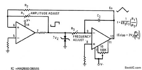
PROGRAMMED_FUNCTION_GENERATOR
Published:2009/7/2 21:21:00 Author:May
View full Circuit Diagram | Comments | Reading(587)
Simple_voltage_doubler
Published:2009/7/24 0:34:00 Author:Jessie

This circuit doubles available battery voltage using an LTC1044 switched-capacitor voltage converter. The circuit will drive low-power 74-CMOS (3-to 15-V) equipment for extended periods of time from two small 1.5-V cells. Efficiency exceeds 90% for load currents below 1.75 mA. Figure 8-7B shows output voltage versus loading (shown as VOUT=6 V). (View)
View full Circuit Diagram | Comments | Reading(766)
Inductorless_high_current_switching_regulator
Published:2009/7/24 0:33:00 Author:Jessie

This circuit operates from 12-V battery (6 cells), and provides5-V output at 1 A. Notice that no inductor is required. (View)
View full Circuit Diagram | Comments | Reading(557)
Switching_preregulated_linear_regulator_low_noise
Published:2009/7/24 0:31:00 Author:Jessie

This circuit is similar to that of Fig. 8-4, except that the low-dropout series regulator at switching-regulator output serves to eliminate switching-induced noise. The circuit also operates from a 9-V battery and will supply 25-mA of noise-free, regulated power with short-circuit current set by the FET 30-mA IDSS. (View)
View full Circuit Diagram | Comments | Reading(943)
LOGIC_PROBE
Published:2009/7/2 21:21:00 Author:May

Provides almost as much information, when working with TTL or DTL digital circuits, as costly CRO or logic analyzer. Can be built into length of plastic tubing, with probe tip projecting at one end and two supply leads coming from other end.One LED flashes for high to low transition, and other for low to high transition. Flash is visible even with very narrow pulses, because probe circuit stretches pulse width. With S1 open (memory mode), pulse LED at right stays on until reset by operator, for capturing any stray pulse. If probe tip is held on open circuit or on chain of floating inputs, no LED will light.-C. W. Andreasen, Superprobe, 73 Magazine, Holiday issue 1976, p 92-93. (View)
View full Circuit Diagram | Comments | Reading(2937)
60_Hz_HIGH_Q_NOTCH
Published:2009/7/2 21:19:00 Author:May
Input network for SN72310 voltage-follower opamp provides at-tenuation of 60-Hz power-line frequency. Use high-quality capacitors for maximum a.- The Linear and Interface Circuits Data Book for Design Engineers, Texas Instruments, Dallas, TX, 1973, p 4-39. (View)
View full Circuit Diagram | Comments | Reading(591)
SUMMING_AMPLIFIER
Published:2009/7/2 21:18:00 Author:May
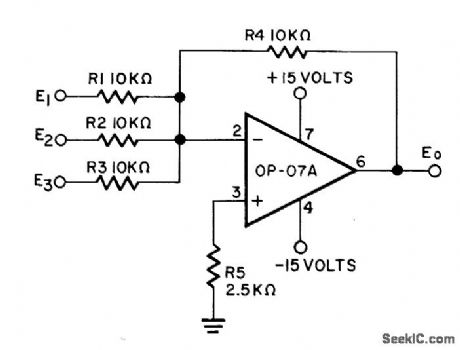
Provides output equal to sum of all input voltages. with high precision. Use of Precision Monolithics OP-07A opamp makes circuit adiustment-free.- Ultra-Low Offset Voltage Op Amp. Precision Monolithics. Santa Clara. CA. 1977. OP-07. p 7. (View)
View full Circuit Diagram | Comments | Reading(0)
LOW_DISSIPATION_1_MC_FLIP_FLOP
Published:2009/7/24 1:42:00 Author:Jessie

Complementary-pair circuit keeps power dissipation below 2 mw, with standby power of only 150 microwatts. Consists of two interconnected flip-lops, sharing common diode steering network at input. Diodes D1, D4, D5, and D8 protect emitter-based junctions from breakdown and also increase switching speed by clamping back bias levels at base of transistor. May be used for binary operation, as staler, or as shift register.-M. E. McGee and J. H. Wujek Jr., One-Megahertz Flip-Flop Saves Standby Power, Electronics, 39:12, p 106-107. (View)
View full Circuit Diagram | Comments | Reading(687)
Current_mode_SMPS_controllers
Published:2009/7/24 1:41:00 Author:Jessie

Figure 7-40 shows the MAX741D connected to provide +5 V at 1.5 A or 3.0 A with a 6-V to 15.5-V input. Figure 7-41 shows the MAX741D connected to provide +5 V at 1 A from a +3-V input. Both configurations are SMPS (switch-mode power supplies). The data sheet shows how the MAX741 can be programmed to provide different outputs with supply voltages from 2.7 V. MAXIM NEW RELEASES DATA Book, 1994, P. 4-131. (View)
View full Circuit Diagram | Comments | Reading(788)
HIGH_IMPEDANCE_DIFFERENTIAL_VTVM
Published:2009/7/24 1:41:00 Author:Jessie

Infinite input impedance is obtained in direct.coupled d-c amplifier by continuously and automatically feeding back to input a bucking voltage equal to signal voltage. Use of both inputs permits differential easurements of small signal voltages at mean levels between -150 and +300 v, for measuring grid-cathode potentials in high-impedance circuits or for balancing high-impedance push-pull circuits. Instead of input voltage dividers, range resistors are used in output circuit. Voltage supply need not be regulated.-V. D. Schurr, D-C Amplifier Expands Input Voltage Range, Electronics, 31:23, p 87-89. (View)
View full Circuit Diagram | Comments | Reading(492)
SCR_AND_LAMP_DISPLAY_CONTENTS_OF_REGISTER
Published:2009/7/24 1:40:00 Author:Jessie

Computer register lo be sampled is connected to input A, and input B is fed with 10-microsec, 12-V positive pulse. When output of register is at its low level of -12 V, diode D1 conducts but D2 does not, so scr D3 is nonconducting and lamp is off. When register output is high level (ground potential), coincident positive voltages applied to base of scr make it conduct and turn lamp on. -J. J. Collins, Displaying the Contents of a Computer Register, Electronics, 37:21, p 72. (View)
View full Circuit Diagram | Comments | Reading(610)
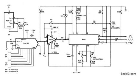
DAC_CONTROLLED_FUNCTION_GENERATOR
Published:2009/7/2 21:18:00 Author:May
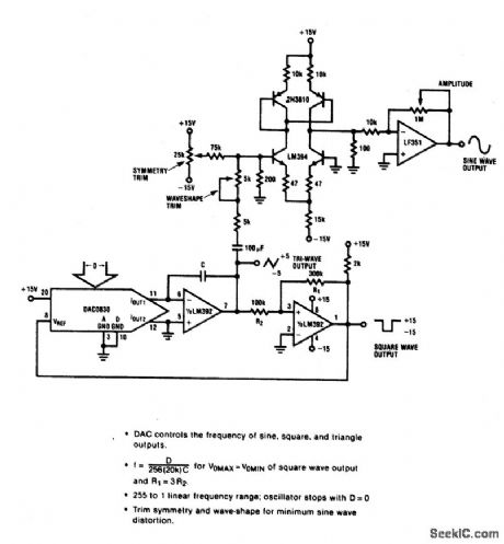
View full Circuit Diagram | Comments | Reading(587)
FET_LOGIC_PROBE
Published:2009/7/2 21:15:00 Author:May
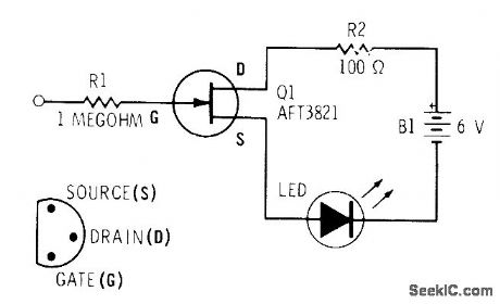
Field-effect transistor with very high input resistance makes LED glow when logic 1 is present at input, without loading circuit being monitored.-F. M. Mints, Computer Circuits for Experimenters, Radio Shack, Fort Worth, TX, 1974, p 35-43. (View)
View full Circuit Diagram | Comments | Reading(653)
Square_root_V_F_converter
Published:2009/7/24 1:39:00 Author:Jessie

Fig, 12-27 This circuit generates an output frequency proportional to the square root of the input voltage. IC1 serves as a divider and V/F converter. The IC1 output goes back to the denominator input through IC2 (connected as a F/V converter) to make the circuit output equal to the input square root. The 5-kΩ scale-factor trim is adjusted for a full-scale output of 10 kHz. National Semiconductor Linear Applications Handbook 1991 p 1309. (View)
View full Circuit Diagram | Comments | Reading(563)
| Pages:1133/2234 At 2011211122112311241125112611271128112911301131113211331134113511361137113811391140Under 20 |
Circuit Categories
power supply circuit
Amplifier Circuit
Basic Circuit
LED and Light Circuit
Sensor Circuit
Signal Processing
Electrical Equipment Circuit
Control Circuit
Remote Control Circuit
A/D-D/A Converter Circuit
Audio Circuit
Measuring and Test Circuit
Communication Circuit
Computer-Related Circuit
555 Circuit
Automotive Circuit
Repairing Circuit