
Circuit Diagram
Index 1131
20_dB_GAIN_FOR_2m
Published:2009/7/2 22:10:00 Author:May

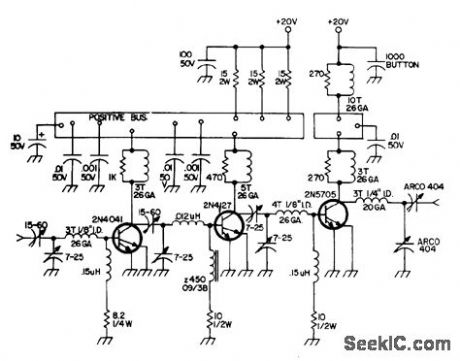
Input of 200 mW is amplified to 20 VV. Positive 20-V sources are separated so final stage can be amplitud-modulated; for FM, connect to single supply.Transistors require heatsinks.-Circuits, 73 Magazine, May 1973, p 106. (View)
View full Circuit Diagram | Comments | Reading(438)
SPEECH_RECOGNITION_FILTER
Published:2009/7/2 22:07:00 Author:May

Voice signal picked up by microphone is preamplified and sent through 3-kHz low-pass passive filter C1-R1 to 1-kHz high-pass active filter and 1-kHz low-pass active filter using sections of LM3900 quad opamp. Diode symbols on opamps indicate use of current mirrors for noninverting inputs. Outputs are sampled about 60 times per second to implement speech recognition algorithm of computer, which counts number of high-pass and low-pass zero crossings per second and compares results with series of word models in memory to determine most likely match.-J. R. Boddie, Speech Recognition for a Personal Computer System, BYTE, July 1977, p 64-68 and 70-71. (View)
View full Circuit Diagram | Comments | Reading(2356)
1_kHz_FIFTH_ORDER_LOW_PASS
Published:2009/7/2 22:06:00 Author:May

Uses single first-order section and two different second-order sections to give passband gain of 10.3 dB,Opamps can be 741 or equlvalent,-H,M.Berlin, Design of Active Filters, with Experments, Howard W,Sams, Indianapons, IN,1977,p 119-122. (View)
View full Circuit Diagram | Comments | Reading(955)
Q_MULTIPLlER
Published:2009/7/2 22:05:00 Author:May
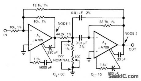
Alticle glves design procedure and equations for utilking Q multiplication to simplify circuit for active bandpass filter,With values shown,center frequency is 3.6 kHz and Q of10 is multiplied by gain of 6 to give effective Q of 60.-A, B,Williams, Q-MultipIier Techniques Increase filtor Selectivity,EDN Magazine,Oct 5,1975,p74 and 76. (View)
View full Circuit Diagram | Comments | Reading(615)
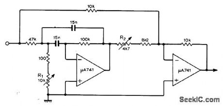
TUNABLE_NOTCH_FILTER
Published:2009/7/2 22:03:00 Author:May

Simple pot-tuned active notch filter has tuning range of 200 Hz in audio band and 3-dB rejection bandwidth of 10 Hz, as required for tuning out whistle or powerline hum that is interfering with radio program.Article gives design theory for many other types of notch filters.-Y. Nezer, Activ (View)
View full Circuit Diagram | Comments | Reading(0)
TUNABLE_NOTCH
Published:2009/7/2 22:01:00 Author:May
Opamp circuit requires only one pot (R1) to vary notch frequency. R2 is used to set noise rejection to maximum. With values shown, filter tunes from 170 Hz to 3 kHz, with 3-dB bandwidth of 230 Hz and notch rejection better than 40 dB over entire range. Circuit can be voltage-tuned by replacing R, with FET operated as voltage-variable resistor.-R. J.Harris, Simple Tunable Notch Filter, Wireless World, May 1973, p 253. (View)
View full Circuit Diagram | Comments | Reading(653)
DARLINGTON_LOGIC_PROBE
Published:2009/7/2 22:01:00 Author:May

Two-transistor Darlington connection provides very high input impedance that does not load logic circuit being monitored, while driving LED that glows when logic 1 is present at input.-F. M. Mims, Computer Circuits for Experimenters, Radio Shack, Fort Worth, TX, 1974, p 35-43. (View)
View full Circuit Diagram | Comments | Reading(1786)
BUILT_IN_LOGIC_PROBE
Published:2009/7/2 21:58:00 Author:May
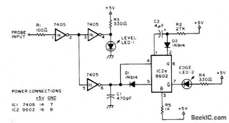
PROBE-Permanently wired LEDs indicate TTL levels and changes in levels, LEVEL LED-1 comes on for TTL 1 input and goes out for TTL 0 input. EDGE LED-2 comes on momentarily for input changes. Will detect levels, steps, single pulses, and pulse trains. Only haif of each IC is used, so dual tester can be made if desired. ICs 1a and 1b form noninverting driver for 9602 mono which is triggered on both positive-going and negative-going edges by C1 and D1. Pulse train input having period less than width of flash pulse will keep EDGE indicator on.-K. W. Christner, The Built-In Logic Tester, BYTE, Jan. 1977, p 82-83. (View)
View full Circuit Diagram | Comments | Reading(506)
TEMPERATURE_COMPENSATED_OFFSET_CONTROL
Published:2009/7/2 21:54:00 Author:May

Drift effects of offset adjustment are removed by deriving correction current from emitter-base voltage of PNP signal transistor to develop appropriate temperature compensatioll. Correction current is divided with conventional control pot used for adjusting offset voltage. Article gives design equations.-J.Graeme, Offset Null Techniques Increase Op Amp Drift, EDN Magazine. Aprill. 1971. p 47-48. (View)
View full Circuit Diagram | Comments | Reading(658)
1_kHz_THREE_FUNCTION
Published:2009/7/2 21:50:00 Author:May
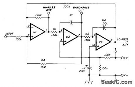
Uses National LM324 quad opamp, with appropriate biasing for single supply of +5 to +25 VDC. Values of R1 and R2 establish fc at 1000 Hz, while R3 gives Q of 50. Values of R1 and R2 for other bandpass center and cutoff frequencies fc can be calculated from R = 15 ×107/fc. Fourth opamp may be used as output amplifier or for summing highpass and low-pass outputs. C1 is same as C2.-P. A. Lovelock, Discrete Operational Amplifier Active Filters, Ham Radio, Feb. 1978, p 70-73. (View)
View full Circuit Diagram | Comments | Reading(647)
LOGIC_PROBE
Published:2009/7/2 21:49:00 Author:May

Pocket-size battery-powered probe using two inexpensive CMOS ICs has such low standby current drain that ON/OFF switch is unnecessary. Drain is appreciable only when LEDs are on during use. Mallory TR-133 4.2-V mercury battery gives 2-V threshold for TTL compatibility. LEDs come on to indicate logic 1. Pulse-stretching circuit ensures detecting positive or negative pulses as short as 250 ns.-J. Edrington, Battery-Powered Logic Probe Needs No ON/OFF Switch, EDN Magazine, May 20, 1975, p 72 and 74. (View)
View full Circuit Diagram | Comments | Reading(0)
R_F_VOLTMETER
Published:2009/7/24 1:32:00 Author:Jessie
Circuit generates low-frequency waveform whose amplitude is equivalent to that of unknown r-f voltage, using photochopper modulator VI-V2 as error detector. Arrangement gives seven voltage ranger from 10 my rms to 10 v rms full scale, over frequency range of 500 kc to 1,000 Mc.-T. C. Anderson, Measuring Low-Level R-F Voltage with Servo Feedback Techniques, Electronics, 34:28, p 63-65. (View)
View full Circuit Diagram | Comments | Reading(839)
SHAFT_POSITION_MODULATOR
Published:2009/7/24 1:31:00 Author:Jessie

Used for modulating and mixing 1.5-kc data carrier and 600-cps ready signal in system for trans.mitting digitally encoded master shaft positions over phone line at 750 bits per sec and.-R. B. Palmiter, Digital System Positions Shafts Over Phone Line, Electronics, 32:7, p 62-66. (View)
View full Circuit Diagram | Comments | Reading(486)
PREFERRED_INSTRUMENT_SERVO_MOTOR_CONTROLLER
Published:2009/7/24 1:30:00 Author:Jessie

Used to excite control winding of 2-phase Mark 7 Mod 1 and Mark 14 Mod 0 servo motors. Delivers nominal output of 1 W to loads with effective resistance between 2,000 and 4,000 ohms. Maximum output is 50 V. CR1 is 75-ma silicon recliner with 70-V reverse working voltage.-NBS, Hand-book Preferred Circuits Navy Aeronautical Electronic Equipment, Vol. I, Electron Tube Circuits, 1963, PC 70, p 70-2. (View)
View full Circuit Diagram | Comments | Reading(752)
Low_power_switching_regulator
Published:2009/7/24 0:30:00 Author:Jessie

This circuit provides 5-V output from a 9-V source with 80% efficiency and 50-mA output capability. The circuit is short-circuit protected. (View)
View full Circuit Diagram | Comments | Reading(520)
Low_dropout_regulator
Published:2009/7/24 0:29:00 Author:Jessie

This circuit provides both a +12-V and a +5-V output from a single 6-V battery, with very low dropout (Fig.8-3B). Quiescent current is 760 μA, and the100-mA output is short-circuit protected (see chapter 4 for testing). (View)
View full Circuit Diagram | Comments | Reading(1208)
High_current_battery_splitter
Published:2009/7/24 0:27:00 Author:Jessie
This circuit can source or sink up to ±150 mA with only 5 mA quiescent current. The value of C2 can be increased as necessary to absorb current transients. (View)
View full Circuit Diagram | Comments | Reading(573)
Micropower_battery_splitter
Published:2009/7/24 0:26:00 Author:Jessie

This circuit provides symmetrical ±output voltages, both equal to one-half the input voltage (one 9-V battery in this case). The output voltages are referenced to pin 3 (output common). The circuit will operate with other battery voltages. If the battery exceeds 6 V, pin 6 should also be connected to pin 3, as shown by the dashed line. (View)
View full Circuit Diagram | Comments | Reading(578)
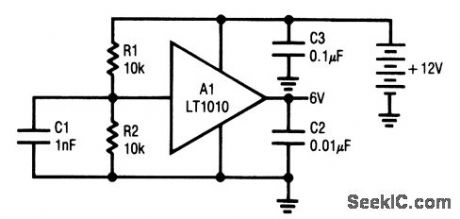
Ultra_low_noise_wideband_preamplifier
Published:2009/7/24 0:25:00 Author:Jessie

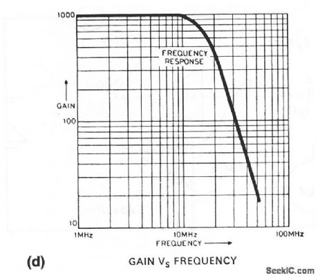
The ZN459/CP used in this circuit is a high-gain low-noise preamplifier designed for audio/video applications at frequencies up to 15MHz. Figures 2-7B and 2-7C show typical PC board layouts for the ZN459 and ZN459CP (DIP), respectively .Figure 2-7D shows gain versus frequcncy. (View)
View full Circuit Diagram | Comments | Reading(840)
Improved_three_terminal_regulator_for_high_voltages
Published:2009/7/24 0:22:00 Author:Jessie


This circuit is an improved version of the circuit in Fig. 7-67. (View)
View full Circuit Diagram | Comments | Reading(567)
| Pages:1131/2234 At 2011211122112311241125112611271128112911301131113211331134113511361137113811391140Under 20 |
Circuit Categories
power supply circuit
Amplifier Circuit
Basic Circuit
LED and Light Circuit
Sensor Circuit
Signal Processing
Electrical Equipment Circuit
Control Circuit
Remote Control Circuit
A/D-D/A Converter Circuit
Audio Circuit
Measuring and Test Circuit
Communication Circuit
Computer-Related Circuit
555 Circuit
Automotive Circuit
Repairing Circuit