
Circuit Diagram
Index 1136
NEGATIVE_R
Published:2009/7/2 20:51:00 Author:May
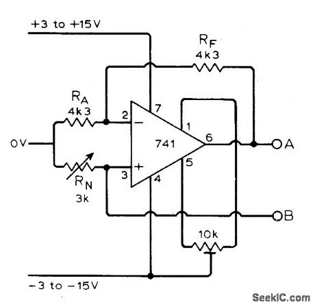
Negative-resistance connection of 741 opamp is suhable for both AC and DC applications. Requires floating power supply because 0-V terminal floats with respect to both output terminals. For DC use, adjust 10K pot to cancel offset voltage of amplifier. Value of negative resistance is varied with RN or by adjusting ratio of RF to RA. Can be used to make LC circuits operate at subaudio frequencies.-D. A. Miller. Negative Resistor. Wireless World. June 1974. p197. (View)
View full Circuit Diagram | Comments | Reading(666)
LOW_COST_ADJUSTABLE_FUNCTION_GENERATOR
Published:2009/7/2 20:45:00 Author:May

This low-cost operational-amplifier circuit (A) generates four different functions with adjustable periods. For the components shown here, the period of the output waveforms is given by T = 4RC and T = 2RC. With switch S1 in position A,V1 is a triangular waveform,while V2 is a square wave (B). With the switch in position B,a sawtooth waveform is generated at V1 and a pulse at V2 (C). (View)
View full Circuit Diagram | Comments | Reading(649)
TONE_TIMBRE_DEMONSTRATOR
Published:2009/7/24 2:08:00 Author:Jessie
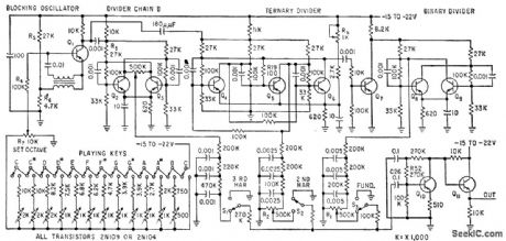
Demon-strates principles of Fourier synthesis of musical tone, for one octave. Lowest fundamental is 250 cps. Switches S1, S2, and S3 add or remove third harmonic, second harmonic, or fundamental components from out put signal to change tone quality. Master oscillator has range of 1.5 to 3 kc. Blocking oscillator Q1 is tuned through one octave by varying voltage to which R4 is returned, by switching resistors in series with playing keys.-W. S. Pike and C. N. Hoyler, Synthesizing Timbre for Electronic Musical Tones, Electronics, 32:22, p 92-94. (View)
View full Circuit Diagram | Comments | Reading(537)
500_Hz_LOW_PASS_UNITY
Published:2009/7/2 20:44:00 Author:May
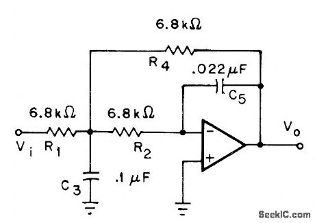
GAIN-Multiplefeedback filter using 741 or equivalent opamp has unity gain in passband below 500-Hz cutoff.Resistors can be 5% tolerance.-H. M, Berlin, Design of Active Filters, with Experiments, Howard W. Sams, Indianapolis, IN,1977,p 99-1O0. (View)
View full Circuit Diagram | Comments | Reading(757)
SELF_INDICATING_REGISTER
Published:2009/7/24 1:52:00 Author:Jessie

Combines two self-indicating flip-flops with phase splitter that converts single-polarity shift pulses to positive and negative-going pulses for all stages. Indicator triodes are Amperex 6977.-H. Rodriques de Miranda and I. Rudich, Indicator Triode for Direct Data Readout, Electronics, 33:6, p 52-54. (View)
View full Circuit Diagram | Comments | Reading(539)
LATCHING_ALARM
Published:2009/7/2 20:43:00 Author:May

Single-channel monitorusing half of CD4013AE flip-flop detects out-of-tolerance condition or alarm state representedby logic 1 on dockinput Flip-flop then changesto alarm state that turns on transistor for energizing alarm device,and holds alarm condition until operator reacts by applying voltage to SET input,Logic 0 on D terminal activates flip-flop when monitoring is desired.-J,C Nichols,CMOS D Flop Makes Latching AND Gate.EDN Magazine,April 20, 1974,p 89 and 91. (View)
View full Circuit Diagram | Comments | Reading(0)
1_kHz_SIXTH_ORDER_HIGH-PASS
Published:2009/7/2 20:43:00 Author:May
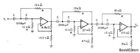
Formed by cascading three different second-order sections,Passband gain is 12.5 dB Opamps can be 741 or equivaient Used when high reiection is needed for signals just below passband,in application where such rejection justifies cost of extra filter sections.-H. M. Berlin, Design of Active Filters,with Experiments, Howard W Sams, Indianapolis, IN 1977, p 122-125. (View)
View full Circuit Diagram | Comments | Reading(960)
Basic_F_V_converter_1
Published:2009/7/24 1:51:00 Author:Jessie

Fig. 12-33 This circuit uses an XR4151 and a few external components to form a basic F/V converter. Using the values shown, the input frequency is from 0 to 10 kHz, and output voltage is from 0 to 10 V. It might be necessary to square up the input signals. Also, the values for the input differentiator can be altered to accommodate square-wave inputs of different amplitudes and frequencies. EXAR Corporation Databook, 1990.p. 5 124. (View)
View full Circuit Diagram | Comments | Reading(1837)
1_PPS_CLOCK_GENERATOR
Published:2009/7/24 1:51:00 Author:Jessie

Uses unique magnetic shift register in which elements are connected in rings, with output of first element connected to input of first. Each ring has own driver, all operated from same 400-cps pulse generator.-J. H. Porter, Miniaturized Autopilot System for Missiles, Electronics, 33:43, p 60-64. (View)
View full Circuit Diagram | Comments | Reading(1212)
Precision_V_F_converter
Published:2009/7/24 1:50:00 Author:Jessie

Fig. 12-32 This circuit is similar to that of Fig. 12-31, except that the additional op amp permits the circuit to retain linearity over the full range of input voltage, all the way to 0 V. Trim the full-scale adjust pot so that a 10-V input produces a 10-kHz output. Then, set the offset-adjust pot for 10 Hz with an input of 10 mV. EXAR Corporation Databook, 1990, p 5-124 (View)
View full Circuit Diagram | Comments | Reading(670)
CMOS_DRIVER_FOR_OPAMP
Published:2009/7/2 20:43:00 Author:May
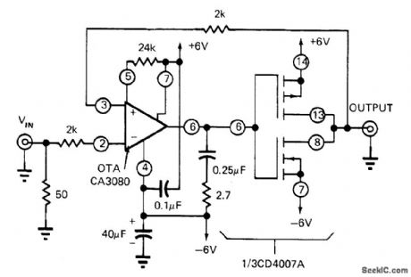
CMOS inverterpalr(one-third of CD4007A) iS used in closedloop mode as unity-gain voltage follower for CA3080 opamp .Slew rateis 1 V/μS Output current capability of 6 mA can be increased by paralleling two other sections of CMOS.-B Furlow.CMOS Gates in Linear Applications: The Results Are Surprisingly Good.EDN Magazlne.March 5.1973.p42-48. (View)
View full Circuit Diagram | Comments | Reading(770)
SIMPLE_FET_VOLTMETERS
Published:2009/7/24 1:50:00 Author:Jessie

Uses single active device to indicate full scale at 1 v input, for sensitivity of 1 meg per volt. Bias is at 300 microamp drain current, approximately point of zero drift.-L. J. Sevin, Jr., Field-Effect Transistors, McGraw-Hill, N.Y., 1965, p 109. (View)
View full Circuit Diagram | Comments | Reading(613)
2000_SEC_COUNTER
Published:2009/7/24 1:50:00 Author:Jessie

Up to 20 and gate in-puts can be supplied by each closed ring element. 1-pps clock triggers operate 2,000-sec counter pulse generator using unique magnetic shift register elements.-J. H. Porter, Miniaturized Autopilot System for Missiles, Electronics, 33:43, p 60-64. (View)
View full Circuit Diagram | Comments | Reading(527)
1_kHz_HIGH_PASS_UNlTY
Published:2009/7/2 20:42:00 Author:May
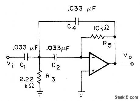
GAlN-Passband gain of 741 or equivalent opamp circuit is set by ratio of C4 to C1 rather than by resistors. Values shown give unity gain for passband above 1-Hz cutoff. Circuit uses multiple feedback.-H. M.Berlin, Design of Active Filters, with Experiments, Howard W. Sams, Indianapolis, IN, 1977, p 100-102. (View)
View full Circuit Diagram | Comments | Reading(578)
PRECISION_A_C_VOLTMETER
Published:2009/7/24 1:49:00 Author:Jessie

Measures a-c voltages between 95 and 135 v with 0.6% accuracy while using ordinary 2% accuracy meter. Zener diodes provide reference voltage.-D. S. Belanger, Simple Circuit Increases Measurement Accuracy, Electronics, 38:22, p 69. (View)
View full Circuit Diagram | Comments | Reading(616)
OCTAVE_AUDIO_EQUALIZER
Published:2009/7/2 20:42:00 Author:May
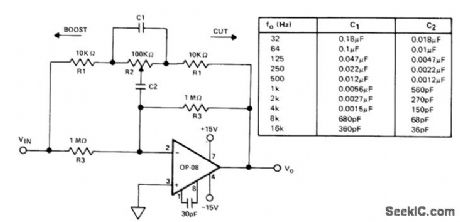
R2 provides up to 12-dB boost or cut at center frequency determined by values of C1 and C2 as given in table.Uses Precision Monolithics OP-08 opamp. Low input bias current of opamp permits scaling resistors up by factor of 10, to reduce values of C1 and C2 at low-frequency end. Same circuit is used for all 10 sections of equalizer, which together draw only 6 mA maximum from supply.- Precision Low Input Current Op Amp, Precision Monolithics, Santa Clara, CA, 1978, OP-08, p 1. (View)
View full Circuit Diagram | Comments | Reading(649)
2-kHz_LOW-PASS
Published:2009/7/2 20:40:00 Author:May
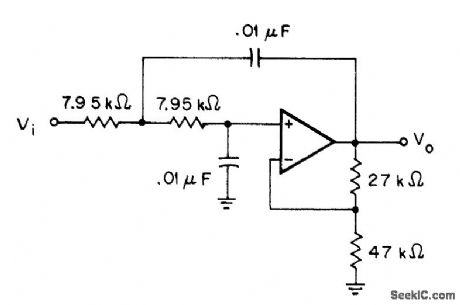
Voltage-contralled voltagesource filter uses equal-value input resistorsand equal-value capacitors, simplifying selection of components Equation for cutoff froquency then simplifies to f=1/6.28RC or 1/(6.28)(7950)(0.01)(10-6) Opamp can be 741.-H.M.Berlin, Design of Active Filters,With Experiments, Howard W.Sams,Indianapolis,IN,1977,p 85-86. (View)
View full Circuit Diagram | Comments | Reading(652)
1_MHz_TRACKING_FILTER
Published:2009/7/2 20:38:00 Author:May

Exar XR-S200 PLLIC is connected to function as frequency filter when phase-locked loop locks on input signal, to produce filtered version of input signal frequency at VCO output. Because circuit can track input over 3:1 range of frequencies around freerunning frequency of VCO, it is known as tracking filter. Optional wideband discriminator output is also provided.- Phase-Locked Loop Data Book, Exar Integrated Systems, Sunnyvale,CA,1978, p 9-16. (View)
View full Circuit Diagram | Comments | Reading(794)
LOW_PASS_AF
Published:2009/7/2 20:36:00 Author:May
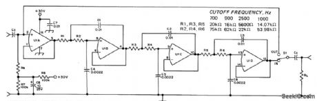
Can be used to attenuate un desired high-frequency audio response in superhet or direct-conversion receivers having inadequate IF selectivity, to improve CW or SSB reception. Resistor values determine cutoff frequency; 700 and 900 Hz are for CW and 2500 Hz for SSB. Insert filter at point having low audio level. Filter has input buffer, three cascaded active low-pass filter stages, and IN/OUT switch.Overall gain is unity. U1 is Fairchild μA4136, Raytheon RC4136, or equivalent quad opamp.Overall response is 1.5 dB down at cutoff frequency, about 36 dB down at twice cutoff, and about 60 dB down at three times cutoff. R7 and R8 provide pseudoground of half supply voltage, to eliminate need for negative supply. Will operate with supply from 6 to 36 V, drawing about 7 mA.-T, Berg, Active Low-Pass Filters for CW or SSB, QST, Aug. 1977, p 40-41. (View)
View full Circuit Diagram | Comments | Reading(914)
ECL_INTERFACE_FOR_LED
Published:2009/7/2 20:35:00 Author:May

PNP germanium transistor serves as interface for driving LED from emitter-coupled logic. Same interface can be used to drive 7-segment or other arrays that have common-cathode configuration, such as Fairchild FND10 or Monsanto MAN3. Optoisolator can be used in place of LED.-G. A. Altemose, One Transistor Provides ECL to LED lnterface, EDN Magazine, Oct. 15, 1972, p 54, (View)
View full Circuit Diagram | Comments | Reading(677)
| Pages:1136/2234 At 2011211122112311241125112611271128112911301131113211331134113511361137113811391140Under 20 |
Circuit Categories
power supply circuit
Amplifier Circuit
Basic Circuit
LED and Light Circuit
Sensor Circuit
Signal Processing
Electrical Equipment Circuit
Control Circuit
Remote Control Circuit
A/D-D/A Converter Circuit
Audio Circuit
Measuring and Test Circuit
Communication Circuit
Computer-Related Circuit
555 Circuit
Automotive Circuit
Repairing Circuit