
Circuit Diagram
Index 1126
ELECTROMYOGRAM_AMPLIFIER
Published:2009/7/3 2:09:00 Author:May
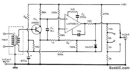
Used to amplify voltages in range of several microvolts to several millivolts in frequency spectrum of 20 to 5000 Hz, as picked up with 13-mm thin silver disks placed on skin over muscle being studied.Article also covers electrocardiographin applications involving source impedances as high as 50 kilohms (as with one electrode on each wrist). Maximum output capability is 9 V P-P.Voltage gain is 1000. RF is 800K pot, ad lusted to give 12 dB per octave dropoff above turnover frequency.-R. E. George, Simple Amplifier for Muscle Voltages, Wireless World, Oct. 1972, p 495-496. (View)
View full Circuit Diagram | Comments | Reading(1061)
STEREO_MULTIPLEXER
Published:2009/7/24 3:15:00 Author:Jessie

F-m retention is monaural when 19-kc multiplex input is absent or below acceptable power level. Rectification of 19-kc signal provides turn-on voltage to frequency doubler, for stereo.-S. Messin and T. E. Nawalinski, A Solid Stale Stereo Set Built in Modules, Electronics, 38:16, p 88-92. (View)
View full Circuit Diagram | Comments | Reading(560)
FET_SIEREO_FM_TUNER
Published:2009/7/24 3:14:00 Author:Jessie

Uses four tuned r-f circuits, two in high-Q highly selective band. pass filter, plus two fet r-f stages in addition to fet mixer and local oscillator. Agc voltage for the two gain-controlled fet r-f stages is derived front fourth i-f stage, which also drives narrow-band meter amplifier.-F. L. Mergner, P-i-n Diode and FET's Improve F-M Reception, Electronics, 39:17, p 114-1 18. (View)
View full Circuit Diagram | Comments | Reading(1414)
12_V_ynreset_output_high_efficiency_controller_non_boot_strayaped
Published:2009/7/24 3:14:00 Author:Jessie

Figure 7-70 shows a MAX770/71/72 connected to provide 12-V output at 0.5 A, with a 5-V input. See Fig. 7-68 for component suppliers. This non-boot-strapped version of the Fig. 7-69 circuit requires less supply current, but with the full 5-V input. Use the Fig. 7-69 controller for input voltages less than 5 V. MAXIM NEW RELEASES DATA Book, 1995, P. 4-15. (View)
View full Circuit Diagram | Comments | Reading(528)
Micropower_thermometer
Published:2009/7/24 3:10:00 Author:Jessie

Fig. 13-41 The output of this circuit is a current proportional to temperature, which can be used to drive a meter for a direct readout. Alternatively, a resistor or op amp can be used to get a voltage output. The circuit is pulsed at a low duty cycle to reduce power consumption. With the component shown, the duty cycle is about 0.2% with a one-second sample rate. This gives an average current drain of about 25μA, plus the output current. The circuit will operate with a supply of 8.0 to 12.0 V. A small 8. 4-V mercury battery can provide an operating life of about one year. R8 is used to trim the circuit, correct for Zener tolerance, temperature error in the sensor, and resistor tolerance. With the values shown, a 0- to 50-μA output is obtained for a +50 to + 100°F temperature change. Other ranges can be selected using the equations shown in the box on the circuit diagram. The current-source output allows long lines to be driven with no loss of accuracy. National Semiconductor Linear Applications Habdbook, 1991, p. 1229.
(View)
View full Circuit Diagram | Comments | Reading(1)
Relative_humidity_sensor
Published:2009/7/24 2:34:00 Author:Jessie

Fig, 13-20 This circuit combines two LTC1043 switched-capacitor building blocks with a capacitive-based humidity transducer (Parametrics #RHS) to provide full signal conditioning for a relative-humidity output. To calibrate, place the sensor in a known 5% relative-humidity environment, and adjust the 10-kΩ 5% RHtrim for a 0.05-V output. Next, place the sensor in a 90% relative-humidity environment and set the 500-Ω 90% RH trim for 900-mV output. Repeat this procedure until both points are fixed. Once calibrated, this circuit is accurate within 2%on the 5 to 90%alative-humidity range.Linear Technology Linear Applications Handbook, 1990.
(View)
View full Circuit Diagram | Comments | Reading(842)
16_BIT_WORD_GENERATOR
Published:2009/7/24 2:34:00 Author:Jessie
Provides all possible 16-bit serial binary words at 10-Mc rate, to simulate expected input of high-speed computer circuits. Four identical binary stages are used in word generator. Speed is derived from high-transconductance tetrodes.-R. G. Norquist, Testing High-Speed Digital Computer Circuits, Electronics, 32:29, p 50-51. (View)
View full Circuit Diagram | Comments | Reading(748)
SCR_PREREGULATOR_FITS_ANY_POWER_SUPPLY
Published:2009/7/3 2:06:00 Author:May

Circuit Notes
This SCR pre-regulator keeps the filter capacitor Vc, in a variable output power supply, a few volts above the output voltage Vo. The benefits include: less heat dissipated by the pass transistor and therefore small heatsink, cooler operation and higher efficiency, especially at low output voltages.Q1, R1, R2, D1 and D2 form a constant current source for zener Z1, so that the contribution to the output current is always a few mA (2-3 mA).The Darlington pair Q2, Q3 keeps the SCR off. The voltage Vcdecreases until Vc= Vo=V at which point the Darlington pair fires the SCR, charging the filter capacitor to a higher voltage Vc1 in less than half the period of the input voltage. The component values, shown are for a 0-250-V, 3-A power supply. (View)
View full Circuit Diagram | Comments | Reading(1)
300-MHz_complementary_amplifier_56-V_supply
Published:2009/7/24 2:33:00 Author:Jessie

The electrical characteristics for the 2N5160 and 2N3866 shown in this circuit are given in Fig.2-23B and 2-13B,respectively. (View)
View full Circuit Diagram | Comments | Reading(1132)
BINARY_TONE_GENERATOR_FOR_BLIND
Published:2009/7/3 2:05:00 Author:May
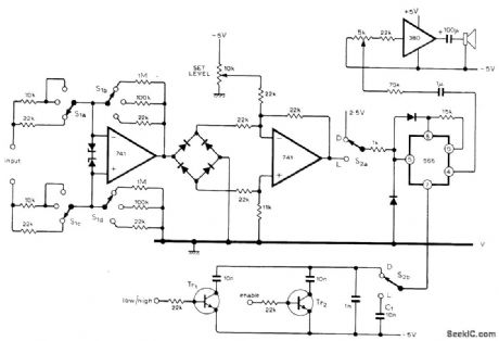
When low/high input is voltage in binary form, as obtained from converter circuit (also given in artide) fed by digital voltmeter, circuit produces Iow pitch for binary 0 and high pitch for binary 1 when S2 is set at D for digital voltmeter mode. Recognition of binary digits in tone form can be leamed by blind person much as leaming of Morse code. Uses LM566 IC as tone-generating VCO that feeds loudspeaker through LM380 IC amplifier and 5K volume control. With S2 at position L, circuit serves as audio null detector for bridge connected to input terminals; S1 is used to increase sensitivity of 741 opamp as null is approached. Article covers operation of circuits in detail.-R. A. Hoare, An Audible Voltmeter and Bridge-Indicator, Wireless World, Sept.1976, p 87-89. (View)
View full Circuit Diagram | Comments | Reading(1671)
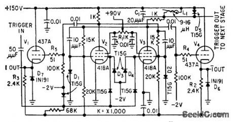
WELD_TEMPERATURE_CONTROL
Published:2009/7/24 2:29:00 Author:Jessie

Welding voltage passes through transformer for synchronous rectification to give signal for operational amplifier V1-V2. Output, which is integral of difference between command voltage and resistive input voltage, is used to provide correct, fusion temperature under varied welding conditions.-G. R. Archer, Feedback and NOR Logic Yield Sound Spot Welds, Electronics, 33:8, p 48-51. (View)
View full Circuit Diagram | Comments | Reading(587)
DEMODULATOR_WITH_CARRIER_DETECT
Published:2009/7/3 1:56:00 Author:May

Exar XR-567 PLL system is used with XR-215 FM demodulator to detect presence of carrier signal in narrow-band FM demodulation applications where bandwidth is Iessthan 10% of carrierfrequency. Output of XR-567 is used to turn off FM demodulator when no carrier is present, giving squelch action. Circuit will detect presence of carrier up to 500 kHz.- Phase-Locked Loop Data Book, Exar Integrated Systems, Sunnyvale, CA, 1978, p 41-48. (View)
View full Circuit Diagram | Comments | Reading(1154)
SENSING_MUSCLE_TENSION
Published:2009/7/3 1:55:00 Author:May
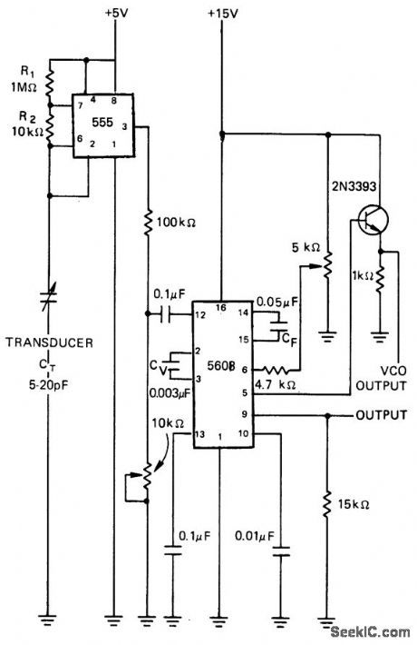
Capacitive transducer of type used for measuring displacement and pressure is used to modulate 555 MVBR. Frequency is detected in NE560B PLL that produces DC output voltage. CF sets bandwidth of demodulated information. Zero-position frequency of transducer is measured at pin 12 of PLL, and VCO frequency of PLL is measured from pin 5 through 2N3393 emitter-follower stage.-R. M. Wise, Capacitive Transducer Senses Tension in Muscle Fibers, Electronics, June 26, 1975, p 97; reprinted in Circuits for Electronics Engineers, Electronics, 1977, p 349. (View)
View full Circuit Diagram | Comments | Reading(605)
HIGH_GAIN_D_C_PREAMP_FOR_VTVM
Published:2009/7/24 1:49:00 Author:Jessie

Use of current source as load resistor of Q2 minmizes battery supply effect on zero selling. Additional current source Q5-R3-D3-D4 serves in place of common-emitter resistance for Q1-Q2 to reduce sensitivity to negative supply voltage excursions and boost open-circuit gab above 300. Preamp will extend 1.5-v range down to 500, 150, and 50 my full-scale for voltage measurements in semiconductor circuits without damaging transistors.-A. K. Scidmore, Low-Cost Emitter-Follower Extends Voltmeter's Range, Electronics, 39;3, p 87. (View)
View full Circuit Diagram | Comments | Reading(664)
Off_line_regulator_with_adjustable_output
Published:2009/7/24 0:07:00 Author:Jessie

In this circuit, the two regulators are connected in series to increase the voltage capability. However, neither regulator exceeds its maximum differential voltage-even under short-circuit conditions. (View)
View full Circuit Diagram | Comments | Reading(640)
3_A_positive_adjustable_voltage_regulator_1
Published:2009/7/24 0:06:00 Author:Jessie


The LLM is a three-terminal adjustable regulator IC with an output range from +1.2 to +32 V, with the output voltage set by two external resistors. Because the regulator is floating, higher output voltages can be obtained as long as the maximum input-output differential is not exceeded. Characteristics are shown in Fig. 7-60B, 7-60C, and 7-60D. (View)
View full Circuit Diagram | Comments | Reading(656)
Compandor_with_90_dB_range_and_power_down_mute
Published:2009/7/24 0:04:00 Author:Jessie

This NE/SA578 circuit is similar to that of Fig.1-34,except that the programmable dynamic range is 90 dB. (View)
View full Circuit Diagram | Comments | Reading(505)
LINE_FM_DEMODULATOR
Published:2009/7/3 1:50:00 Author:May

Exar XR-2212 predsion PLL IC provides Iinear demodulation for both narrow-band and wideband FM signals. Article gives circuit design procedure.With +12 V supply voltage and 67-kHz carrier frequency having ±5 kHz frequency deviation, R0 is 18K fixed resistor in series with 5K pot. C0 (between pins 13 and 14) is 746 pF, R1 is 89.3K, C1 is 186 pF, RF is 100K, and RC is 80.6K. These values give ±4 V P output swing. AII values except R0 can be lounded off to nearest standard value.- Phase-Locked Loop Data Book, Exar Integrated Systems, Sunnyvale, CA, 1978, p 35-40. (View)
View full Circuit Diagram | Comments | Reading(1940)
AURAL_TACTILE_METER_FOR_BLIND
Published:2009/7/3 1:47:00 Author:May

Converts DC input voltage in range of 0-100mV into audible indication that is produced at instant when measured voltage exceeds reference voltage as set by decade switches of R7. Blind person can then read Braille markings at switch settings to get input voltage. Opamp B is connected as free-running MVBR that generates AF signal for earpiece. Use germanium transistors such as OC45 or OC71. Opamps are Motorola 1435.Use silicon diodes such as 1N914,BA100、or OA200 R7 can alternatively be wirewoundpot,-R.S. Maddevel.Meterfor Blind Students,Wireless World.Jan.1973.p36-37. (View)
View full Circuit Diagram | Comments | Reading(748)
DIRECT_COUPLED_AMPLIFIER
Published:2009/7/24 1:46:00 Author:Jessie
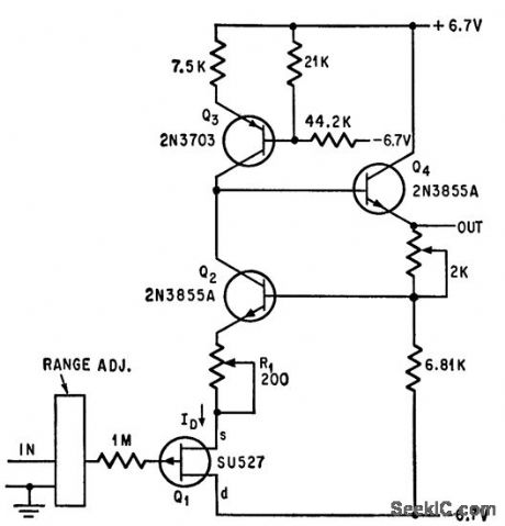
Gives high input impedance and low drift at low cost, with approximately unity gain. Uses one fet and three bipolar transistors. Suitable for d-c voltmeter having 0.1 v full scale on lowest range. Temperature drift is low.-J. M. Colwell, Direct-Coupled Amplifier Cuts Cost of D-C Voltmeter, Electronics, 39:12, p 109-110. (View)
View full Circuit Diagram | Comments | Reading(1413)
| Pages:1126/2234 At 2011211122112311241125112611271128112911301131113211331134113511361137113811391140Under 20 |
Circuit Categories
power supply circuit
Amplifier Circuit
Basic Circuit
LED and Light Circuit
Sensor Circuit
Signal Processing
Electrical Equipment Circuit
Control Circuit
Remote Control Circuit
A/D-D/A Converter Circuit
Audio Circuit
Measuring and Test Circuit
Communication Circuit
Computer-Related Circuit
555 Circuit
Automotive Circuit
Repairing Circuit