
Circuit Diagram
Index 1125
AF_LOW_PASS_FOR_CW
Published:2009/7/3 2:20:00 Author:May

Design using 10% tolerance components gives sufficiently wide bandwidth while maintaining steep skirt re sponse for CW reception in direct-conversion communication receiver. Filter has five identical three-transistor sections, each peaked at cutoff frequency. a of each section is about 1.9, which gives 6-dB bandwidth of about 200 Hz. With center frequency at 540 Hz attenuation is 75 dB at 1200 Hz. Net gain of system is 28 dB at resonance. NPN transistors are 2N3565,2N3904, or similar; PNP transistors are 2N3638, 2N3906, or similar.-W. Howard, Simple Active Filters for Direct-Conversion Receivers, Ham Radio, April 1974, p 12-15. (View)
View full Circuit Diagram | Comments | Reading(987)
TUNABLE_FOURTH_ORDER_LOW_PASS
Published:2009/7/3 2:19:00 Author:May

Use of four ganged pots permits varying cutoff frequency over 10:1 range. Table gives ranges obtainable with five different values for C.Opamps can be 741 or equivalent. Tracking of 5% for pots calls for expensive components, but ordinary snap-together pots may prove satisfactory if tuning range is restricted to 3:1 or less and more capacitor switching is used.-D. Lancas.ter, Active-Filter Cookbook, Howard W.Sams,Indianapolis, IN, 1975, p 195-197. (View)
View full Circuit Diagram | Comments | Reading(736)
Single_chip_audio_amplifier_BTL_stereo_1_W
Published:2009/7/23 23:58:00 Author:Jessie
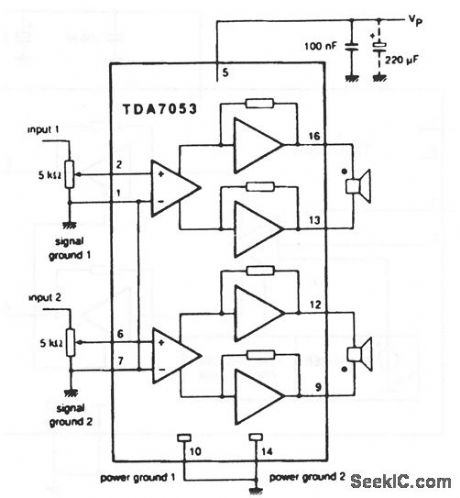
This circuit is similar to that of Fig. 1-27, except that no built-in volume control is provided, and two (stereo) channels are available. The supply range is from 3 V to 18 V. The circuit provides a 1-W per channel output, with a 6-V supply, into 8-Ω stereo loads, or 2-W per channel output, with an 11-V supply, into 25-Ω loads. Fixed, closed-loop voltage gain is 39 dB (6-V supply, 8-Ω load). (View)
View full Circuit Diagram | Comments | Reading(834)
24_kHz_LOW_PASS_HIGH_PASS
Published:2009/7/3 2:18:00 Author:May

Three 741 opamps are connected toprovide separate low-pass and high-pass outputs simultaneously for complex synthesis problem requirIng state-variable filter Gain is 1.-D,Lancaster, Active-Filter Cookbook, Howard W,Sams,Indianapolis,IN,1975, p 192-193. (View)
View full Circuit Diagram | Comments | Reading(773)
TWO_PENTODE_MIXER
Published:2009/7/23 23:58:00 Author:Jessie

Combines range markers and radar video. Compensated load improves high-frequency response.-NBS, Handbook Preferred Circuits Navy Aeronautical Electronic Equipment, Vol. 1, Electron Tube Circuits, 1963, p N4-4. (View)
View full Circuit Diagram | Comments | Reading(628)
Loopback_tests
Published:2009/7/23 23:57:00 Author:Jessie


Figure 3-Q shows a loopback test circuit for the MAX3241. Figures 3-R and 3-S show the loopback test results at 120 kbps and 240 kbps, respectively. Notice that the input is applied at the transmitter input, and that both the transmitter output (connected to receiver input) and the receiver output waveforms are monitored. (View)
View full Circuit Diagram | Comments | Reading(767)
5_A_negative_adjustable_voltage_regulator
Published:2009/7/23 23:57:00 Author:Jessie


The LAS79HG is four-terminal adjustable-regulator IC with an output range from -2.6 to 30 V, providing remote sensing from a single pot. Characteristics are shown in Fig. 7-56B and 7-56C. (View)
View full Circuit Diagram | Comments | Reading(747)
1_kHz_HIGH_PASS_FLATTEST_RESPONSE
Published:2009/7/3 2:17:00 Author:May

Values are chosen for flattest possible response obtainable with third-order configuration of two 741 opamps. Tripling capacitance values cuts cutoff frequency by one-third and vice versa. Component tolerance can be 10%. Gain is 2.-D.Lancaster, Active-Filter Cookbook, Howard W. Sams, Indianapolis, IN, 1975, p 186. (View)
View full Circuit Diagram | Comments | Reading(496)
Basic_F_V_converter_with_cascade_transistor
Published:2009/7/23 23:57:00 Author:Jessie

Fig. 12-22 This circuit is similar to that of Fig. 12-19, but with a cascade transistor at the output to improve nonlinearity to 0.006% (typical). Again, set the 5-kΩ gain adjust for 10-V output with a 10-kHz input. National Semiconductor, Linear Applications Handbook 1991 p 1299. (View)
View full Circuit Diagram | Comments | Reading(736)
Smgle_chip_audio_amplifier_BTL_mono_1_W_2_W
Published:2009/7/23 23:57:00 Author:Jessie
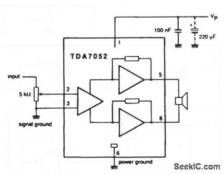
This circuit is similar to that of Fig. 1-27, except that no built-in volume control is provided. The supply range is from 3 V to 18 V. The circuit provides an output of 1W, with a 6-V supply, into an 8-Ω load, or 2-W output when the supply is raised to 11 V, into a 25-Ω load. Fixed, closed-loop voltage gain is 39 dB (6-V supply, 8-Ω load). (View)
View full Circuit Diagram | Comments | Reading(631)
TWO_PENTODE_RADAR_AND_IFF_MIXER
Published:2009/7/23 23:57:00 Author:Jessie

Each grid is clamped by diode to establish base line of positive input pulse at -1.8 v.-NBS, Handbook Preferred Circuits Navy Aeronautical Electronic Equipment, Vol. 1, Electron Tube Circuits, 1963, p N4-5. (View)
View full Circuit Diagram | Comments | Reading(619)
Single_chiyo_audio_amplifier_BTL_1_W_05_W_with_volume_control
Published:2009/7/23 23:56:00 Author:Jessie
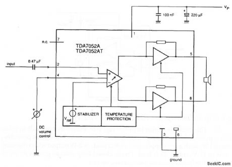
This circuit makes use or the bridge-tied load (BTL) principle to achieve low-voltage operation without sacrifice of output power. The wide supply range (4.5 V to 18 V) makes the circuit suitable for a broad range of applications (battery-powered radios, telephone sets, etc.). The IC amplifier has a built-in dc volume control, with a log characteristic range of more than 80 dB.When the dc control voltage (pin 4) drops below 0.3 V, the amplifier is muted, so there are no switch-on/switch -off clicks. The TDA7052A provides an output of 1 W with a 6-V supply into an 8-Ω load, or 2-W output when the supply is raised to 12 V, into a 32-Ω load. The TDA7052AT output is 0.5 W with a 6-V supply, into a 16-Ω load. Basic amplifier circuit titles and descriptions (View)
View full Circuit Diagram | Comments | Reading(658)
AUDIBLE_VOLTMETER
Published:2009/7/3 2:17:00 Author:May
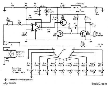
Voltage-controlled audio oscillator produces 400-Hz tone for 0 V, with frequency of tone increasing with voltage overtwo-octave rangeto 1600 Hz for maximum or full-scale voltage. Ten-resistor voltage divider produces calibrated reference tones corresponding to main 0-10 divisions of meter scale foraural comparison. Simple square-wave audio oscillator Q1-Q2 is voltage-controlled by Q3, which in turn is driven by opamp whose gain is set by R5. Article covers adjustment of sensitivity pot R5, and frequency pots R24-R33 so VCO tracks voltage being measured and tones coincide at MONITOR and COMPARE positions of S1 for each meter division.-H. F. Batie, An Audible Meter for the Blind Amateur, CQ, Dec. 1973, p 26-31. (View)
View full Circuit Diagram | Comments | Reading(3)
8_A_positive_fixed-current_regulator_with_remote_sensing
Published:2009/7/23 23:56:00 Author:Jessie

This circuit uses the LAS3905 IC (Fig. 7-50) as a fixed current regulator with remote sensing. Characteristics are shown in Fig.7-50B, 7-50C, and 7-50D. (View)
View full Circuit Diagram | Comments | Reading(551)
Basic_F_V_converter_with_passive_filter
Published:2009/7/23 23:56:00 Author:Jessie

Fig. 12-21 This circuit is similar to that of Fig. 12-19, but with a passive filter added to reduce ripple. Typically, ripple is less than 1 mVp-p for frequencies from 200 Hz to 10 kHz. Again, set the 5-kΩ gain adjust for 10-V output with a 10-kHz input. National Semiconductor, Linear Applications Handbook 1991.p 1298. (View)
View full Circuit Diagram | Comments | Reading(588)
ZENER_DIODE_INCREASE_FIXED_PNP_REGULATOR’S_OUTPUT_VOLTAGE_RATINGS
Published:2009/7/3 2:12:00 Author:May

Circuit Notes
A zener diode in the ground lead of a fixed pnp regulator varies the voltage output of that device without a signiftcant sacriftce in regulation. The technique also allows the regulator to operate with output voltages beyond its rated limit. (View)
View full Circuit Diagram | Comments | Reading(929)
225_MHz_FRONT_END_
Published:2009/7/3 2:11:00 Author:May
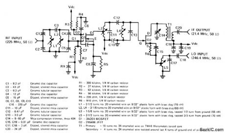
RF stage, mixer, and tuned circuits are designed for use in FM communication receiver having local oscillator input of 246.4 MHz, for IF of 21.4 MHz .Supply voltage is 12.5 V. Spurious-response rejecti is 100 dB, image rejection is 97 dB, and noise figure is 12 dB.-J. Hatchett and B. Morgan, Economical 225 MHz Receiver Front End Em ploys FETs, Motorola, Phoenix, AZ, 1978, EB22. (View)
View full Circuit Diagram | Comments | Reading(1639)
RADAR_AND_BEACON_MIXER
Published:2009/7/23 23:56:00 Author:Jessie

Two pentodes combine two inputs into single output.-NBS, Handbook Preferred Circuits Navy Aeronautical Electronic Equipment, Vol. 1, Electron Tube Circuits, 1963, p N4-5. (View)
View full Circuit Diagram | Comments | Reading(644)
_5_V_500_mA_step_douon_converter_module
Published:2009/7/23 23:56:00 Author:Jessie


Figure 7-24 shows a MAX1738 2.5-W converter module that requires no extemal components. Figure 7-25 shows the pin descriptions and operating characteristics. The no-load current is 1.7 mA, with 60-μA shutdown current. Ripple is a typical ±30 mV, which can be improved using the optional output filter of Fig. 7-26. MAXIM NEW RELEASEs DATA BOOK, 1994, P. 4-23, 4-25, 4-26.
(View)
View full Circuit Diagram | Comments | Reading(550)
VOLTAGE_REGULATOR
Published:2009/7/3 2:10:00 Author:May

View full Circuit Diagram | Comments | Reading(0)
| Pages:1125/2234 At 2011211122112311241125112611271128112911301131113211331134113511361137113811391140Under 20 |
Circuit Categories
power supply circuit
Amplifier Circuit
Basic Circuit
LED and Light Circuit
Sensor Circuit
Signal Processing
Electrical Equipment Circuit
Control Circuit
Remote Control Circuit
A/D-D/A Converter Circuit
Audio Circuit
Measuring and Test Circuit
Communication Circuit
Computer-Related Circuit
555 Circuit
Automotive Circuit
Repairing Circuit