
Circuit Diagram
Index 1124
VACUUM_TUBE_AUDIO_AMPLIFIER_POWER_SUPPLY
Published:2009/7/24 4:04:00 Author:Jessie

A suitable power supply that provides isolation from the 120-Vac line is shown. The circuit uses two filament transformers connected back to back. The secondary voltages can be almost any value, as long as they are equal. A 1:1 isolation transformer can be substituted, if available. The transformers should be rated at least 25 VA or more. (View)
View full Circuit Diagram | Comments | Reading(699)
10_Hz_LOW_PASS
Published:2009/7/3 2:31:00 Author:May

Filter design for biomedical experiment has 10-Hz cutoff, tolerable transient and overshoot response, and at least 30-dB rejection of all frequencies above 15 Hz. All components should have 2% tolerance.-D. Lancaster, Active-Filter Cookbook, Howard W.Sams, lndianapolis, IN, 1975, p 147. (View)
View full Circuit Diagram | Comments | Reading(1049)
FORCED_SWITCHING
Published:2009/7/24 4:03:00 Author:Jessie

Bypassing of emitter-follower with inductor L cuts normal 70-nsec switching time to 38 nsec. Use of diode D across L improves rise time without affecting fall lime.-T. Asai, Forced-Switching Emitter Follower, EEE, 12:2, p 29. (View)
View full Circuit Diagram | Comments | Reading(534)
AUDIO_EMG_MONITOR
Published:2009/7/3 2:29:00 Author:May

Used to measure very small voltages that appear on surface of skin over body muscle. Instead of recording voltage in form of electromyogram (EMG), opamp drives transistor circuit to produce audible note that varies in pitch as EMG signal varies in amplitude. Applications include use by stroke patient as aid to leaming reuse of muscle group affected by stroke. Q1 rectifies and averages amplified EMG signal. Q2 controls charging current of C5 for varying frequency of UJT oscillator Q3.-R. Melen and H. Garland, Understanding IC Operational Amplifiers, Howard W. Sams, Indianapolis, IN, 2nd Ed., 1978, p 125-127 (View)
View full Circuit Diagram | Comments | Reading(2016)
Magnetic_speed_switch_signal_conditioner
Published:2009/7/24 4:03:00 Author:Jessie
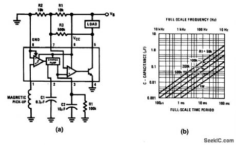
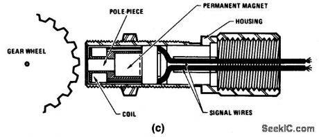
Fig. 14-17 This circuit uses an LM2907 as a signal conditioner for a magnetic speed switch, where the load is energized only when the input frequency exceeds a value set by R1 and C1. A typical example is an anti-pollution device included on recent automobiles. The device disables the vacuum-advance function until a certain speed is attained. A typical automotive pickup (Fig. 14-17C) provides 1000 pulses per mile so that, at 60 mph, the incoming frequency is 16.6 Hz. If the reference level is set by two equal resistors, R1 and R2, then the desired value of C1 and R1can be found from the equation VCC/2 VCC x C1 x R1 x f,C1R1f 0.5, and C1R1=0.03. From the RC selection chart (Fig. 1417B) choose suitable values for C1 and R1 (0.3 μF and 100 kΩ, for example). The circuit will then switch (load energized) at about 60 mph. National Semiconductor Linear Applications Handb00k 1990 p. 427. (View)
View full Circuit Diagram | Comments | Reading(1683)
VARIABLE_Q_AF
Published:2009/7/3 2:28:00 Author:May


Consists of tuned amplifier having inverse feedback, connected so bandwidth at -6 dB is variablefrom 50 to 400 Hz for center frequency of 1 kHz. Improves selectivity of amateur receivers. Audio from receiver is applied to inverter Q3 through Q1. Part of inverted signal is fed back to twin-T network R1-R2-R3-C1-C2-C3 which has high impedance to ground except at its resonant frequency. Unattenuated signal goes through Q2 for adding to uninverted output at base of Q3. Degree of cancellation by two out-of-phase signals feeding Q3 is controned by R4 to adjust selectivity Filtered output is boosted by Q4 and Q5,Article covers construction,calibration,and operation,Q1-Q6 are GE-20,and Q7 is GE-14 or GE-28,-c,Townsend,A Variable Q Audio Fillter,73 Magazine,Feb,1974, p 54-56. (View)
View full Circuit Diagram | Comments | Reading(626)
ONE_CHIP_BURGLAR_ALARM
Published:2009/7/3 2:27:00 Author:May

The single-chip, burglar-alarm circuit shown uses a dual 556 timer, draws 10 mA of standby current, and generates a pulsing alarm signal that conserves battery energy. Once activated, the alarm will remain on, independent of the subsequent state of any of the sensors. The sensors support both deferred and immediate-action modes. You can attach this circuit to your car's internal lighting circuitry using a single wire and a relay. To arm this circuit, you open your car door and close switch SA. The switch discharges capacitor C4 and holds the timer (one half of the 556 IC) in a reset state to prevent false triggering while you're arming the circuit. When you close your car door, the circuit enters a standby mode. If the door is then reopened, the sensors apply a negative-going pulse to trigger 1. Output 1 then increases, enabling the alarm for 1.1RlC1 seconds. Output 1's high state triggers the multivibrator, the other half of the 556, which begins to cycle after a delay equal to 1.1 (R2 + R3) C2 seconds. As long as the timer's output stays high, the multivibrator will continue to cycle, turning the horn off and on at 3.3-second intervals. During the interval between time that the timer's output increases and the time that the multivibrator's output decreases, you can disarm this circuit using switch SA. To prevent false triggering caused by switch contacts, at S1, S2, and S3, that may bounce when closing the door, make the R6C3 time constant as large as possible. In addition, capacitors C1 and C2 should be tantalum types and should exhibit leakage of less than 1 μA at room temperature.
(View)
View full Circuit Diagram | Comments | Reading(2003)
FAST_ACTION_AT_10_KC
Published:2009/7/24 4:03:00 Author:Jessie

Reverse bias is applied to gate of scr at cutoff to make switch open rapidly. Rise time is 10 microsec and fall time 5 microsec for switching 10 ma at up to 10 kc.-E. L. Dosch, SCR Switch Turns Off With Reverse Bias, Electronics, 38:7, p 88. (View)
View full Circuit Diagram | Comments | Reading(543)
MEMORY_SAVE_ON_POWER_DOWN
Published:2009/7/3 2:25:00 Author:May

Circuit NotesThe auxiliary output powers the memory, while the main output powers the system and is connected to the memory store pin. When power goes down, the main output goes low, commanding the memory to store. The auxiliary output then drops out. (View)
View full Circuit Diagram | Comments | Reading(609)
15_A_positive_adjustable_voltage_regulator_1
Published:2009/7/24 0:03:00 Author:Jessie


The LLM is a three-terminal adjustable regulator IC with an output range from +1.2 to +37V, with the output voltage set by two external resistors. Because the regulator is floating, higher output voltages can be obtained as long as the maximum input-output voltage differential is not exceeded. Characteristics are shown in Fig. 7-59B, 7-59C, and 7-59D. (View)
View full Circuit Diagram | Comments | Reading(875)
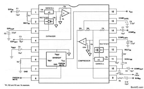
Compandor_with_90_dB_dynamic_range
Published:2009/7/24 0:03:00 Author:Jessie
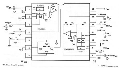
This NE/SA577 circuit is similar to that of Fig. 1-34, except that there is no power-down/mute function, and there is no summing input to the compressor. (View)
View full Circuit Diagram | Comments | Reading(634)
AUTO_ALARM
Published:2009/7/3 2:25:00 Author:May

In operation, the alarm circuit allows a 0-47 second time delay, as determined by the R1/C1 combination, after the switch is armed to allow the vehicle's motion sensor to settle down. This allows you time to get a bag of groceries out of the trunk and not have the hassle of juggling the groceries and the key switch at once.During the time delay, half of LED1, which is actually a single, bi-colored, three-legged common cathode device, lights green. At the same time, pins 8 and 4 of U2 (a 555 oscillator/timer) are held low by U1 (a 3905 oscillator/timer), causing the alarm to remain silent. Once the delay is over, LED1 turns red, indicating that the circuit is armed.At that point, a ground at pin 2 of U2 forces pin 3 of U2 high, closing the contacts of K1 and sounding the siren for a time duration determined by R4 and C2. Once the time has elapsed, pin 3 is pulled low, K1 opens, and the circuit is again ready to go. The circuit can be manually reset by the simple expedient of opening and closing the key switch. Potentiometer R3 controls the LED's illumination intensity. Diode Dl ensures that the green segment of LED1 is fully extinguished when Q1 is turned on-which turns the LED to red. Resistors R4 and R5 must be connected to the +V bus, not to pin 7 of U1, otherwise U2 will mysteriously trigger itself each time the initial delay ends. (View)
View full Circuit Diagram | Comments | Reading(1)
Isolated_RS_485_RS_422_data_interface
Published:2009/7/24 0:02:00 Author:Jessie


Figure 3-1 shows the typical application circuit for the MAX1480A/B. These ICs are complete, electrically isolated RS-485/RS-422 data-communications interfaces. Transceivers, opto-couplers, and a transformer provide a complete interface in one 28-pin package. Figure 3-2 shows the pin descriptions. Figures 3-3 and 3-4 show the function tables. The MAX1408B has reduced-slew-rate drivers that minimize EMI (electromagnetic interference) and reduce reflections caused by improperly terminated cables, allowing error-free data transitions at data rates up to 250 kbps. The MAX1480 driver slew rate is not limited, allowing transmission rates up to 2.5 Mbps. The ICs draw 28 mA of quiescent current. The MAX1408B provides a low-power shutdown mode that consumes only 0.2μA. The drivers are short-circuit current-limited and are protected against excessive power dissipation by thermal shutdown circuits that place the driver outputs into a high-impedance state. The receiver input has a fail-safe feature that guarantees a logic-high output if the input is open circuit. The ICs typically can withstand 1600 Vrms for one minute or 2000 Vrms for one second. MAXIM NEW RELEASES DATA BOOK, 1995, P. 2-13, 2-15, 2-17 (View)
View full Circuit Diagram | Comments | Reading(1786)
Compandor_with_80_dB_dynamic_range_and_power_down_mute
Published:2009/7/24 0:02:00 Author:Jessie
This single-chip NE/SA576 circuit operates on voltages from 1.8 V to 7 V, with a power consumption of 1.4 mA at 3.6V. Multiple external signals can be summed in the compandor at pin 9. The gain level can be programmed by the selection of resistors R1, R2, and R3. If the supply is less than 2 V, connect 20-kΩ resistors between Vcc and VREF, and between VREF and ground (so that the IC will turn on with a 1.8-V supply). The power-down/mute function (pin 8) requires an open-collector signal, and is active-low. (View)
View full Circuit Diagram | Comments | Reading(776)
PITCH_AND_YAW_CHANNELS
Published:2009/7/24 0:01:00 Author:Jessie

Identical channels amplify, demodulate, and shape gyro signal to feed direct-coupled differential servo amplifier whose output differential cur rent goes to dual-coil hydraulic control valve in rocket.-R. E. King and H. Low, Solid-State Guidance For Able-Series Rockets, Electronics, 33:5, p 60-63. (View)
View full Circuit Diagram | Comments | Reading(607)
18_19_MHz_BANDPASS
Published:2009/7/3 2:25:00 Author:May

Butterwolth bandpass filter, suitable for use with broadband preamp, helps reject out-of-band signals. Filter also protects preamp from signals across response range from broadcast band through VHF. C1 and C2 are mica trimmers. L1 and L2 have 30 turns No. 22 enamel on Amidon T68-6 toroid cores to give 5.1 μH.-D. DeMaw, Beat the Noise with a Scoop Loop, QST, July 1977, p 30-34. (View)
View full Circuit Diagram | Comments | Reading(704)
800_Hz_BANDPASS
Published:2009/7/3 2:24:00 Author:May

Active filter has 800-Hz center frequency for optimum CW reception.Bandwidth is adjustable. Back-to-back diodes provide noise-limiting capability.-U. L. Rohde, IF Amplifier Design, Ham Radio, March 1977, p 10-21. (View)
View full Circuit Diagram | Comments | Reading(999)
1_kHz_FOURTH_ORDER_HIGH_PASS
Published:2009/7/3 2:23:00 Author:May

First section is second-order high-pass filter having gain of 1.2 dB,and second section has gain of 7 dB Opamps are 741 or equivalent.-H.M.Berlin, Design of Active Filters, with Experiments, Howard W. Sams, Indianapolis, IN, 1977, p 116-117. (View)
View full Circuit Diagram | Comments | Reading(1182)
EKG_FM_DEMODULATOR
Published:2009/7/3 2:23:00 Author:May
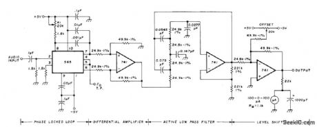


Devel oped as part of system using satellitefor relaying electrocardiograms and other medical data having bandwidth of 0.5 to 50 Hz. Audio signal serving as source of FM is applied to voltage-controlled 1-kHz oscillator having ±40% deviation for fullscale input. Corresponding audio signal at receiving location is fed to input of 565 phaselocked loop. Error voltage of loop, at pin 7, conitains data being sought as well as undesirable DC and AC components. DC component of error signal is removed by 741 differential amplifier following PLL. Following four-pole active RC low-pass filter eliminates high-frequency AC components and determines bandwidth of demodulator. Cutoff frequency is 100 Hz. Final 741 opamp scales and shifts output to reasonable value. Recorded output could not be distinguished from original EKG by doctors.-D. Nelson, Medical Data Relay via Oscar Satellite, Ham Radio, April 1977, p 67-73. (View)
View full Circuit Diagram | Comments | Reading(2467)
INCREASING_THE_POWER_RATING_OF_ZENER_DIODES
Published:2009/7/3 2:21:00 Author:May
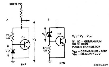
Circuit Notes
A power transistor can be used to provide a high powered zener voltage from a low wattage zener. A 400 mW zener can be used where a 10 watt zener is required or a 1W zener cait be used where a 50 to 80 watt zener is required by using appropriate transistors for Q1 and Q2 in the circuits shown. Where low rating is required, Q1 would be an ASZ 15 (germanium) or an AY9140 (silicon). Q2 could be a 2N2955 (silicon). For higher powers, Q1 should be an ASZ18 (germanium) or a 2N2955 (silicon) and Q2 a 2N3055 (silicon) or an AY8149 (silicon). A heatsink on the transistor is required. The circuit in A has the advantage that power transistors can be bolted directly on to a chassis which may serve as a heatsink. (View)
View full Circuit Diagram | Comments | Reading(2744)
| Pages:1124/2234 At 2011211122112311241125112611271128112911301131113211331134113511361137113811391140Under 20 |
Circuit Categories
power supply circuit
Amplifier Circuit
Basic Circuit
LED and Light Circuit
Sensor Circuit
Signal Processing
Electrical Equipment Circuit
Control Circuit
Remote Control Circuit
A/D-D/A Converter Circuit
Audio Circuit
Measuring and Test Circuit
Communication Circuit
Computer-Related Circuit
555 Circuit
Automotive Circuit
Repairing Circuit