
Circuit Diagram
Index 1127
Typical_RS_485_RS422_network
Published:2009/7/24 1:45:00 Author:Jessie


Figure 3-5 shows the MAX1480A/B connected in a typical RS-485/RS422 network. Figures 3-6 and 3-7 show the layout schematic and PC layout. To minimize reflections, terminate the line at both ends with its characteristic impedance, and keep the stub lengths off the main line as short as possible. The slew-rate-limited MAX1408B is more tolerant of imperfect termination and stubs off the main line. MAXIM NEW RELEASES DATA Book, 1995, P. 2-19, 2-21.
(View)
View full Circuit Diagram | Comments | Reading(2514)
INSTRUMENT_SERVO_CYCLING
Published:2009/7/24 1:32:00 Author:Jessie

Used to cycle instrument servo units from stop to stop for extended periods of time, as for determining wear characteristics and friction level changes. Motor drive is applied so servo pot arm is driven toward +30 v. When 27-V breakdown of D1 is exceeded, it conducts and turns on 1; K1 pulls in, energizing K3, and motor drive reverses. As pot arm approaches -30 V, reversing action occurs again.-P. J. Stein, Instrument Servo Cycling Circuit, EEE, 12:9, p 61. (View)
View full Circuit Diagram | Comments | Reading(575)
OFF_LINE_FLYBACK_REGULATOR
Published:2009/7/3 1:47:00 Author:May
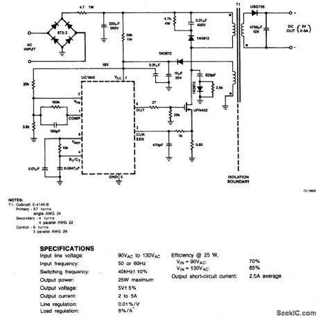
Circuit NotesThis circuit uses a low-cost feedback scheme in which the dc voltage developed from the primary-side control winding is sensed by the UC1842 error amplifier. Load regulation is therefore dependent on the coupling between secondary and control windings, and on transformer leakage inductance. For applications requiring better load regulation, a UC1901 Isolated Feedback Generator can be used to directly sense the output voltage. (View)
View full Circuit Diagram | Comments | Reading(1093)
Three_terminal_regulator_for_high_voltages
Published:2009/7/24 0:13:00 Author:Jessie

This circuit permits regulation of voltages well beyond the range or a three-terminal regulator. Notice that Q2 requires a heatsink because dissipation is 5 W for normal operation, and is possibly 10 W for a short circuit. (View)
View full Circuit Diagram | Comments | Reading(599)
FM_DEMODULATOR_1_
Published:2009/7/3 1:44:00 Author:May
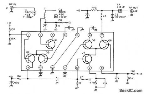
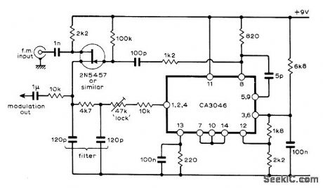
Uses RCA CA3046 IC IF amplifier connected as highly linear voltage-controlled oscillator, in phase-locked loop configuration capableof handling 10.7-MHz amplitude-limited FM input as FM demodulator.Output AF signal is about 20 mV for 75-kHz deviation. FET serves as synchronouschopper type of phase-sensitive detector.-J. L. Linsley Hood, Linear Voltage Controlled Oscillator, Wireless World, Nov. 1973, p 567-569. (View)
View full Circuit Diagram | Comments | Reading(2842)
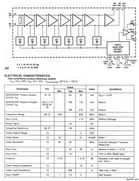
Single_chip_log_amplifier_75_dB
Published:2009/7/24 0:13:00 Author:Jessie
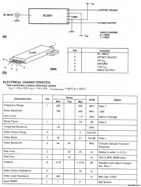
The SL3521 used in this circuit is a successive-detection log amp IC for use in the 100- to 650-MHz range. The IC provides a video output with offset adjust. Figure 2-3B shows the pin connections. Figure 2-3C shows the electrical characteristics. The offset voltage at pin 2 should be in the -0.45- to -0.55-V range, and must not be such as to increase the output offset to more than±0.5 V (View)
View full Circuit Diagram | Comments | Reading(755)
IMPLANT_AMPLIFIER
Published:2009/7/3 1:39:00 Author:May

Designed for use in implanted transmitters monitoring brain and heart potentials. Requires only 4μA at 1.35 V.Voltage gain is 2000, and equivalent input noise only 10 μV P-P with 10-megohm source impedance. Tr1 is current-starved, but resulting limited bandwidth of about 5 kHz is acceptable for biological applications.-C. Horwitz, Micropower Low-Noise Amplifier, Wireless World, Dee. 1974, p 504. (View)
View full Circuit Diagram | Comments | Reading(585)
Three_terminal_regulator_with_minimum_trimming
Published:2009/7/24 0:12:00 Author:Jessie

This circuit is similar to that of Fig. 7-64 and 7-65, but it should not require as much trimming. However, the tolerance is increased to 2%. (View)
View full Circuit Diagram | Comments | Reading(474)
Alternate_three_terminal_regulator_with_trimmable_output_voltage
Published:2009/7/24 0:11:00 Author:Jessie

This circuit is similar to that of Fig. 7-64, except that the resistors are shorted out initially with a jumper. The advantage of this circuit is that VOUT starts lower than the target value, and never exceeds that voltage during the trimming process. Follow the trimming (snipping) procedure shown. (View)
View full Circuit Diagram | Comments | Reading(603)
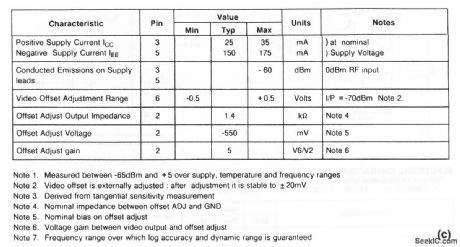
Single_chip_log_limiting_amplifier_75_dB
Published:2009/7/24 0:11:00 Author:Jessie

The SL3522 used in this circuit is a 7-stage successive-detection log amp IC for use in the 100- to 600-MHz range. The IC features an on-chip video amplifier with provision for extemal adjustment of log slope and offset, as well as a balanced RF output. Figure 2-2B shows the electrical characteristics. Compare this single-chip circuit to that of the multi-chip amplifier in Fig. 2-1. (View)
View full Circuit Diagram | Comments | Reading(610)
Three_terminal_regulator_with_trimmable_output_voltage
Published:2009/7/24 0:11:00 Author:Jessie

This circuit performs the same function of that shown in Fig. 7-63, except that a trim pot is not required (some engineers believe that good trim pots are expensive, inexpensive trim pots can be unreliable, and any trim pot that can be adjusted can also be misadjusted). When first tested, this circuit might have a VOUT 4% to 6% higher than the 22.0 V. While monitoring VOUT with a precision meter, snip out R3, R4, and/or R5, as necessary to bring VOUT within 1% of 22.0V. If VOUT is 23.08 V or higher, cut out R3 (if lower, do not cut R3). Then, if VOUT is 22.47 V or higher, cut out R4 (if lower, do not cut R4). Finally, if VOUT is 22.16 V or higher, cut out R5 (if lower, do not cut out R5). (View)
View full Circuit Diagram | Comments | Reading(633)
Wideband_log_IF_strip
Published:2009/7/24 0:10:00 Author:Jessie

This circuit uses 9 SL1613s to produce a successive-detection log IF strip with the characteristics shown. Figure 2-1B shows the pin connections for the SL1613s. (View)
View full Circuit Diagram | Comments | Reading(0)
Three_terminal_regulator_with_small_adjustment_range_trim_pot
Published:2009/7/24 0:08:00 Author:Jessie

This circuit shows how a three-terminal regulator can be trimmed for a specific output voltage over a small range with a trim pot. (View)
View full Circuit Diagram | Comments | Reading(630)
Extending_the_range_of_pnp_three_terminal_regulators
Published:2009/7/24 0:07:00 Author:Jessie

This circuit shows a way to extend the range of a pnp three-terminal regulator. The output voltage equals the regulator voltage plus the Zener voltage. If the Zener is selected to keep the input and ground-pin differential well below the IC breakdown, the input can exceed the maximum rating. For example, a 5-V three-terminal LM2931Z (maximum input 26 V) can become a 56-V regulator with a 51-V Zener. The input can be as low as 56.6 V with a load current of 150 mA or less. (View)
View full Circuit Diagram | Comments | Reading(773)
RADIATION_MONITOR
Published:2009/7/3 1:36:00 Author:May

1N3191 commercial diode serves as sensor in high-accuracy dosagerate meter for gamma rays and high-energy Xrays used in radiotherapy. Diode is small enough for accurate mapping of radiation field.Output voltage varies linearly from 0.1 V to 10 V as dose rate increases from 10 to 1000 rads per minute. Low-drfft FET-input 3521L opamp amplifies detector current to usable level for 3292 chopper-stabilized opamp that provides additional gain while minimizing temperature errors.-P. Prazak and W. B. Scott, Radiation Monitor Has Linear Output, Electronics, March 20, 1975, p 117; reprinted in Circuits for Electronics Engineers, Electronics, 1977, p 106. (View)
View full Circuit Diagram | Comments | Reading(1457)
ACTIVE_ANTENNA_1
Published:2009/7/3 0:01:00 Author:May


All capacitors in this circuit are disc ceramic.Fixed-value resistors are 1/4- or 1/2-W carbon. R1 controls the gain of U1. RFC1 is a miniature 2.5-mH rf choke. T1 has 30 primary turns of #28 enamel wire on an Amidon FT50 -43 ferrite toroid core, and the secondary has four turns of #28 wire. (View)
View full Circuit Diagram | Comments | Reading(750)
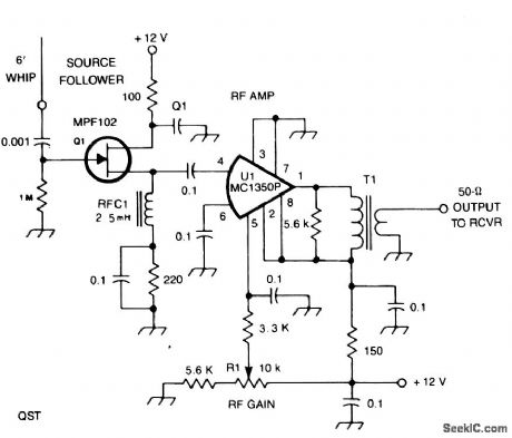
ACTIVE_ANTENNA
Published:2009/7/2 23:55:00 Author:May

Antennas that are much shorter than 1/4 wavelength present a very small and highly relative impedance that is dependent on the received frequency. It is difftcult to match impedances over a decade of frequency coverage. Instead, input stage Q1 is an FET source-follower. A high-impedance input successfully bridges antenna characteristics at any frequency.Transistor Q2 is used as an emitter-follower to provide a high-impedance load for Q1, but more importantly, it provides a low-drive impedance for common-emitter amplifter Q3, which provides all of the amplifter's voltage gain. Transistor Q4 transforms Q3's moderate output impedance into low impedance, thereby providing sufftcient drive for a receiver's 50-Ω, antenna-input impedance. (View)
View full Circuit Diagram | Comments | Reading(2222)
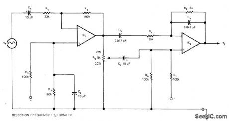
2258_Hz_REJECTION
Published:2009/7/2 23:45:00 Author:May

Provides extremely sharp adjustable-depth notch with only two low-gain opamps. Suitable for single-ended supplies. Article gives equation for transfer function.-R. Carter, Sharp Null Filter Utilizes Minimum Component Count, EDN Magazine, Sept. 20, 1976, p 110.
(View)
View full Circuit Diagram | Comments | Reading(573)
100_kHz_LOW_PASS_UNITY_GAIN
Published:2009/7/2 23:45:00 Author:May
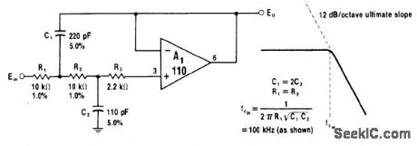
Opamp serves as active element in voltage-controlled voltage-source second-order filter. Other opamps having required high input resistance, low input current, and high speed are 1556 and 8007.-W. G. Jung, IC Op-Amp Cookbook, Howard W. Sams, Indianapolis, IN, 1974, p 331-333. (View)
View full Circuit Diagram | Comments | Reading(505)
VARIABLE_Q_AND_FREQUENCY_1
Published:2009/7/2 23:43:00 Author:May

Bandwidth can be made extremely sharp (less than 9 Hz) or very broad (greaterthan 300 Hz) Adiusting Q to change bandwidth also changes gain of filter.Center frequency of filter is independently adjustable.-A. F. Stahler, An Experimental Comparison of CW Audio Filters, 73 Magazine, July 1973, p 65-70. (View)
View full Circuit Diagram | Comments | Reading(715)
| Pages:1127/2234 At 2011211122112311241125112611271128112911301131113211331134113511361137113811391140Under 20 |
Circuit Categories
power supply circuit
Amplifier Circuit
Basic Circuit
LED and Light Circuit
Sensor Circuit
Signal Processing
Electrical Equipment Circuit
Control Circuit
Remote Control Circuit
A/D-D/A Converter Circuit
Audio Circuit
Measuring and Test Circuit
Communication Circuit
Computer-Related Circuit
555 Circuit
Automotive Circuit
Repairing Circuit