
Circuit Diagram
Index 1128
VARIABLE_Q_AND_FREQUENCY
Published:2009/7/2 23:42:00 Author:May

Bandwidth can be made extremely sharp (less than 9 Hz) or very broad (greaterthan 300 Hz) Adiusting Q to change bandwidth also changes gain of filter.Center frequency of filter is independently adjustable.-A. F. Stahler, An Experimental Comparison of CW Audio Filters, 73 Magazine, July 1973, p 65-70. (View)
View full Circuit Diagram | Comments | Reading(592)
3_kHz_STATE
Published:2009/7/2 23:42:00 Author:May

VARIABLE BANDPASS-Design is based on value of 30 for Q, corresponding to 0.033 for damping factor d. Opamps can be 741.-D. Lancaster, Active-Filter Cookbook, Howard W. Sams, Indianapolis, IN, 1975, p 166. (View)
View full Circuit Diagram | Comments | Reading(712)
AF_NOTCH_1
Published:2009/7/2 23:41:00 Author:May
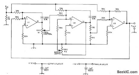
Center frequency of notch can be varied with single control R1; upper limit is about 4 kHz. Circuit Q and notch depth are constant over range. R2 is ad justed initially for best notch depth. All opamps are 741 14-pin DIP,such as Motorola MC1741L. UI and U2 are in-tegrators with DC gain of about 2500, and U3 is summing device. Notch depth is at least 50 dB.may be connected directly across output, or buffer stage can be added to drive lower-impedance loudspeaker or headset. Use with AGC off.-A. Taflove, An Analog-Computer-Type Active Filter, QST, May 1975, p 26-27. (View)
View full Circuit Diagram | Comments | Reading(594)
1_kHz_STATE_VARIABLE_BANDPASS
Published:2009/7/2 23:39:00 Author:May

With three 741 opamps or equivalent, circuit gain is Q (reciprocal of damping). Frequency is changed by changing 10K coupling resistors between opamps while keeping their values equal. Increasing resistors 10 times increases frequency 10 times. High-pass output is obtained from first opamp and low pass from second opamp.-D.Lancaster, Active-Filter Cookbook, Howard W. Sams,Indianapolis, IN, 1975, p 156-159. (View)
View full Circuit Diagram | Comments | Reading(584)
200_400_Hz_PASSBAND
Published:2009/7/2 23:39:00 Author:May

Design is based on use of 3.2 for value of Q, to hold passband dip at 1 dB for two-pole filter. Multiple feedback is used for each pole. First opamp can be 741 or equivalent. Centerfrequency is 283 Hz.-D. Lancaster, Active-Filter Cookbook, Howard W.Sams, Indianapolis, IN, 1975, p 166. (View)
View full Circuit Diagram | Comments | Reading(852)
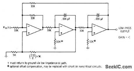
250_Hz_THIRD_ORDER_LOW_PASS
Published:2009/7/2 23:38:00 Author:May

Values shown place cutoff at 250 Hz, with 1-dB dip in response curve. Input must be returned to ground with low-impedance DC path.-D. Lan-caster, Active-Filter Cookbook, Howard W.Sams, Indianapolis, IN, 1975, p 146. (View)
View full Circuit Diagram | Comments | Reading(733)
VOLTAGE_RATIO_METER
Published:2009/7/24 1:45:00 Author:Jessie

Simple circuit, having resolution better than 0.1% for measuring ratio of two voltages, also serves as accurate null detector when difference voltage is less than 0.5 v. A 115-v, 6-w lamp limits voltage applied to meter when differance voltage exceeds 0.5 v. R2 is chosen to give full-scale defection when difference between the two voltages is maximum.-P. A. Lenk, Circuit Permits Accurate Voltage Ratio Measurements, Electronics, 34:52, p 56-57. (View)
View full Circuit Diagram | Comments | Reading(916)
2_METER_IC_RF_AMPLIFIER_
Published:2009/7/2 23:37:00 Author:May
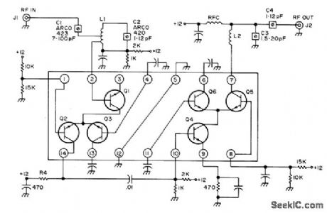
High-gain double compound amplifier using RCA CA3102E haslow noise、 excelle tstabity、 and only twotuned circuits,Ideal for 2-meter FM RF stage,but can be used from DC up to 500 MHz by changing tuned circuits Article covers construction、with emphasis on proper shielding.-B.Hoisington,Two High Gain RF Stages One IC for Two Meter FM 73 Magaze,May 1974,p 47-50 and 52. (View)
View full Circuit Diagram | Comments | Reading(827)
FM_DEMODULATOR_
Published:2009/7/2 23:28:00 Author:May

Uses Signetics NE564 PLL having postdetection processor, operating from 5-V supply. Conversion gain is low so frequency deviation in input signal should be at Ieast 1%.- Signetics Analog Data Manual, Signetics, Sunnyvale, CA, 1977, p 828-830. (View)
View full Circuit Diagram | Comments | Reading(1621)
SUMMING_AMPLIFlER
Published:2009/7/2 23:25:00 Author:May
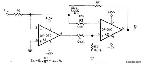
Combination of Precision Monolithics OP-07C and OP-01C opamps gives 18 V/μs slew rate. Can be used as current.output summing amplifier for D/A converter because it requires no zero scale offset adjustments and high speed is preserved.-D. Soderquist and G. Erdi. The OP-07 Ultra-Low Offset Voltage Op Amp-a Bipolar Op Amp That Challenges Choppers. Eliminates Nulling. Precision Monolithics. Santa Clara. CA. 1975. AN-13. p 9. (View)
View full Circuit Diagram | Comments | Reading(725)
OPEN_SHORT_GROUND_ALARM
Published:2009/7/2 23:25:00 Author:May

Pin 6 of CA3094 IC is high for no-alarm condition. When any one sensor line is open, is shorted to other line, or is shorted to ground, output of IC goes low and resulting output current serves for activating alarm system.-E. M. Noll, Linear IC Principles, Experiments, and Projects, Howard W. Sams, Indianapolis, IN, 1974, p 316-317. (View)
View full Circuit Diagram | Comments | Reading(746)
ADD_ON_FM_DETECTOR_
Published:2009/7/2 23:24:00 Author:May

Suitable for any communication receiver. Other IF values can be handled by changing values of L and C. Connecting C2 to pin t0 instead of pin 9 may improve performance. Circuit is easy to construct and align; adjust slug-tuned coil for maximum recovered audio when receMng FM signal.-l. Math, Math's Notes, CQ, April 1975, p 37-38 and 62. (View)
View full Circuit Diagram | Comments | Reading(670)
BEEPER
Published:2009/7/2 23:24:00 Author:May

Intermittent alarm using 555 timer can be set to energize horn, lights, or other signaling device at any desired interval when tripped. When used on auto, sound cannot be mistaken for stuck horn. Choose SCR rating to handle current drawn by relay and timer. If alarm draws less than 200 mA, relay is not needed.-W. Pinner, Alarm! Alarm! Alarm!, 73 Magazine, Feb. 1976,p 138-139. (View)
View full Circuit Diagram | Comments | Reading(824)
20_2000Hz_VARIABLE_BANDPASS
Published:2009/7/2 23:24:00 Author:May

High-Q active bandpass filter can be adjusted over wide frequency range (100:1) while maintaining Q essentially constant over 100. Two-phase output is available. Opamps can be 741 or equivalent. Cascaded all-pass networks B and C each have 0 to 180° phase variation and unity gain at all frequencies, These are driven by opamp A whose feedback signal is sum of input and output of all-pass networks.R2 adjusts Q,andganged log pots change center frequency,-J.M.worley,Variable Band-Pass Filter, Wireless World,April 1977,p 61. (View)
View full Circuit Diagram | Comments | Reading(991)
1_kHz_THIRD_ORDER_HIGH_PASS
Published:2009/7/2 23:22:00 Author:May

Passband gain is 6 dB for Butter worth filter above 1-kHz cutoff Damping factor is 1.000 for both sections,each using 741 or equivalent opamp,-H.M.Berin, Design of Active Filters,with Experiments, Howard w. Sams, Indianapolis, IN,1977,p 115-116. (View)
View full Circuit Diagram | Comments | Reading(858)
VARIABLE_BANDWIDTH_AF
Published:2009/7/2 23:21:00 Author:May
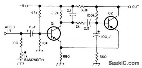
Audio flilter using 1000-Hz Wien bridge provides bandwidths from 70 to 600 Hz Transistors can be SK3004,GE-2,or HEP-254,-Circuits,73 Magazine,Jan,1974,p 124. (View)
View full Circuit Diagram | Comments | Reading(496)
PULSE_FREQUENCY_DETECTOR
Published:2009/7/2 23:20:00 Author:May


Can be usedas digital-logic probe or as frequency detectorfor test equipment,Requires only two ICs,SN7406 hex inverter and SN5400 quad NAND gate. Will respond to square-wave pulses with 50% duty cycles up to 3 MHz. When pulse appears at input, points A and B deteet logic high level and make point E go high so latch sets and tums on LED. Without an inputfrequency, A and B will be complementary and E、will go low,resetting latch and turning off LED.-V, Rende,Digital Frequency Detector Uses Only Two IC's,EON Magazine, April 20,1976,p114. (View)
View full Circuit Diagram | Comments | Reading(2155)
1_kHz_STATE_VARlABLE
Published:2009/7/2 23:20:00 Author:May
Circuit using three 741 opamps offers low sensitivity, voltage-controlled tuning, and easy conversion to high pass or bandpass. For high pass, take output from first opamp. For bandpass, take output from second opamp. To increase frequency, change 10K resistors to identical higher values. 10:1 resistance change produces 10:1 frequency change. Damping d is adjustable; critical value of 1.414 gives maximum flatness of response without overshoot. Design equations are given.-D. Lancaster, Active-Filter Cookbook, Howard W.Sams,Indianapolis, IN, 1975, p129-135. (View)
View full Circuit Diagram | Comments | Reading(538)
TUNING_NULL_INDICATOR
Published:2009/7/2 23:18:00 Author:May

Uses standard left-zero meter as tuning indicator connected in basic opamp AC voltmeter configuration using IC1, with reference buffered by opamp IC2. DC output voltage of tuner is compared with nonzero reference voltage; as these voltages approach each other during tuning, meter pointer moves toward zero, and abruptly reverses direction as tuning null point is passed. Diode D1, protects meter from overload. Use any lowleakage diodes for bridge.-A. S. Holden, Sensitive Null Indicator, Wireless World, Oct. 1974, p 381. (View)
View full Circuit Diagram | Comments | Reading(1344)
Regulated_voltage_up_converter
Published:2009/7/24 1:44:00 Author:Jessie

This circuit improves on the circuit of Fig. 8-7 in that the output remains within about 25 mV of 5 V for loads up to about 2 mA (still using two 1.5-V cells).Figure 8-7B also shows output voltage versus loading (shown as VOUT=5 V). (View)
View full Circuit Diagram | Comments | Reading(551)
| Pages:1128/2234 At 2011211122112311241125112611271128112911301131113211331134113511361137113811391140Under 20 |
Circuit Categories
power supply circuit
Amplifier Circuit
Basic Circuit
LED and Light Circuit
Sensor Circuit
Signal Processing
Electrical Equipment Circuit
Control Circuit
Remote Control Circuit
A/D-D/A Converter Circuit
Audio Circuit
Measuring and Test Circuit
Communication Circuit
Computer-Related Circuit
555 Circuit
Automotive Circuit
Repairing Circuit