
Circuit Diagram
Index 1138
1_kHz_VARIABLE_GAIN_STATE_VARIABLE
Published:2009/7/2 9:23:00 Author:May
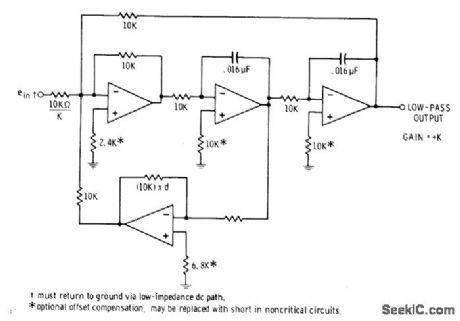
Damping signal is inverted with fourth opamp to make gain and damping as well as frequency independently adjustable. Damping is in range of 0-2, with critical value of 1.414 giving flattest response. For high pass, take output from first opamp; for bandpass, take output from second opamp. Value of input resistor is 10K (10,000 ohms) when gain K is 1.-D. Lancaster, Active- Filter Cookbook, Howard W. Sams, Indianapolis, IN, 1975, p 135-136. (View)
View full Circuit Diagram | Comments | Reading(611)
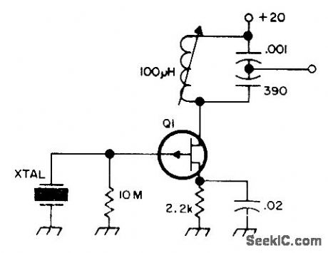
20_100_MHz_OVERTONE_CRYSTAL
Published:2009/7/2 9:23:00 Author:May

Adiustable tank circuit C1L1 ensures operation at desired crystal overtone. Reference voltage for differential amplifier is supplied internally by Motorola 10116 IC and is nominally-1.3 V.-B. Blood, IC Crystal Controlled Oscillators, Motorola, Phoenix, AZ, 1977, AN-417B, P 3. (View)
View full Circuit Diagram | Comments | Reading(985)
TTL_459_MHz_CRYSTAL
Published:2009/7/2 9:22:00 Author:May

Uses FT243 crystat hand-ground to 4.5895 MHz, with 50-pF series capacitor allowing frequency to be trimmed to exactly 4.59 MHz for use in AFSK generator.-J. Nugues, AFSK Generator, Ham Radio, July 1976, p 69. (View)
View full Circuit Diagram | Comments | Reading(789)
1_Hz_WITH_01_Hz_BANDWIDTH
Published:2009/7/2 9:22:00 Author:May

Three pots provides easy trimming to precise values desired. Use R2A to trim bandwidth to exactly 0.100 Hz, Use R1A to trim gain to exactly 10.00.Finally, trim center frequency to exactly 1.000 Hz. Ad justments are almost perfectly noninteracting if made in sequence given.-R. A.Pease, Band-Pass Active Filter with Easy Trim for Center Frequency, Teledyne Philbrick, Dedham,MA,1972, Applications Bulletin 4. (View)
View full Circuit Diagram | Comments | Reading(640)
4_MHz_CRYSTAL
Published:2009/7/2 9:21:00 Author:May

High-stability crystal oscillator usestwo 1500-pF capacitors to swamp out internal lmpedance changes that might cause frequency drift. For best stability when used as frequency standard, choose high-accuracy 4-MHz crystal.-B. Kelley, Universal Frequency Standard, Ham Radilo, Feb. 1974, p 40-47. (View)
View full Circuit Diagram | Comments | Reading(2212)
HYBRID_VIVM
Published:2009/7/24 2:00:00 Author:Jessie

Transistor in each side of balanced vtvm reduces output impedance to fraction of ohm, making meter reading independent of aging of tubes.-J. J. Faran Jr., Hybrid Voltmeter Avoids Aging Errors, Electronics, 36:38, p 41. (View)
View full Circuit Diagram | Comments | Reading(789)
200_MHz_WITH_OSCI_LLATOR_DOUBLER
Published:2009/7/2 9:21:00 Author:May

One section of Motorola MCI0101 is connected as 100-MHz crystal oscillator having crystal in series with feedback loop. LC tank circuit tunes 100-MHz harmonic of crystal and can be used to adjust circuit to exact frequency. Second section of IC serves as buffer and gives complementary 100-MHz signals for frequency doubler having two MC10101 gates as phase shifters and two MC1662 NOR gates. Outputs of MC1662s are wired-OR connected to give 200-MHz signal. One of remaining MC1662 gates is used as bias generator for oscillator.-B. Blood, IC Crystal Controlled Oscillators, Motorola, Phoenix, AZ, 1977, AN-417B, p 5. (View)
View full Circuit Diagram | Comments | Reading(843)
REGISTER_DRIVER
Published:2009/7/24 2:00:00 Author:Jessie

Handles 10-nsee pulses for 50-megapulse computer. Can drive eight 75-ohm lines.-K. H. Konkle and J. E. Laynor, Key to Faster Computers: Ten-Nanosecond Amplifier, Electronics, 35:50, p 39-41. (View)
View full Circuit Diagram | Comments | Reading(748)
Sine_wave_output_converter
Published:2009/7/24 1:59:00 Author:Jessie


This circuit produces a sine-wave output by sequentially switching segments of a 28-V battery stack into a fixed gain, step-up voltage chopper, under digital control. The circuit requires a 14.4-kHz clock. Figure 8-12B shows the voltage presented to the chopper as a function of the sequencing. T1 receives the alternating drive and steps up the voltage. With the values shown, the output is 115 V, 400 Hz, with a power capability of about 20 W. (View)
View full Circuit Diagram | Comments | Reading(704)
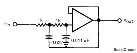
10_Hz_HIGH_PASS_UNITY_GAIN
Published:2009/7/2 9:20:00 Author:May

Low cutoff frequency is 10 Hz in active filter using opamp as voltage-controlled voltage source. Altemative opamps can be 1556 and 8007.-W.Jung, IC OpAmp Cookbook, Howard Sams, Indianapolis, IN, 1974, p 331-333. (View)
View full Circuit Diagram | Comments | Reading(503)
DIFFERENTIAL_FET_VOLTMETER
Published:2009/7/24 1:59:00 Author:Jessie

Two singleended circuits connected back to back give sensitivity of 1 meg/v-L.J. Sevin, Jr., Field-Effect Transistors, McGraw-Hill,N.Y.,1965,p 110. (View)
View full Circuit Diagram | Comments | Reading(733)
TUNNEL_DIODE_SHIFT_REGISTER
Published:2009/7/24 1:59:00 Author:Jessie

Incorporates tunnel-diode steering by Q1 and D1. T1 provides necessary phase reversal.-W. V.Harrison and R. S. Foote, Tunnel Diodes Increase Digital-Circuit Switching Speeds, Electronics, 34:32, p 154-156. (View)
View full Circuit Diagram | Comments | Reading(605)
PEAK_VOLTMETER
Published:2009/7/24 1:58:00 Author:Jessie

Auxiliary flip-flop compares input pulse with voltage already on integrating capacitor. Flip-flop then automatically adjusts capacitor charge to match peak voltage of input. Q2 is integrcaor, controlled by flip-flop Q1-Q2.-R. P. MacKenzie, Novel Design Peak Voltmeter, Electronics, 33:25, p 57. (View)
View full Circuit Diagram | Comments | Reading(795)
SHIFT_REGISTER_DRIVER
Published:2009/7/24 1:58:00 Author:Jessie

Shift pulse input saturates 2N2714, depriving Darlington combination of base drive. Resulting negative pulse generated on 15-V line is differentiated lo produce positive trigger pulse at its trailing edge.- Transistor Manual, Seventh Edition, General Electric Co., 1964, p 432. (View)
View full Circuit Diagram | Comments | Reading(1839)
1_MHz_FET_PIERCE
Published:2009/7/2 9:20:00 Author:May
Field-effect transistor serves in place of vacuum triode in Pierce oscillator. Circuit values are for 1 MHz, but tuned circult can be adjusted to other desired frequency. Q1 can be 2N4360 or T1M12.-Circuits, 73 Magazine, March 1974, p 89. (View)
View full Circuit Diagram | Comments | Reading(652)
STABLE_CRYSTAL
Published:2009/7/2 9:19:00 Author:May

Stability is good enough for microwave transmitter frequency control. Will operate with fundamental or overtone crystals from 1.6 to 160 MHz, whh coils and capacitors being chosen for frequency in use.-Circuits, 73 Magazine, May 1973, p 105. (View)
View full Circuit Diagram | Comments | Reading(1276)
Transceivers_with_external_capacitors_5_V
Published:2009/7/24 1:58:00 Author:Jessie


Figures 3-8 through 3-19 show typical application circuits and pin configurations for the MAX200-MAX211/MAX213. Figure 3-20 shows the selection table for these ICs. Figures 3-21, 3-22, and 3-23 show the control-pin configurations for the MAX200, MAX205/06/11, and MAX213, respectively. Figure 3-24 shows a summary of EIA/TIA-232E, V.28 specifications. Figure 3-25 shows DB9 cable connections commonly used for EIA/TIA-232E and V.24 asynchronous interfaces.These ICs are designed for RS-232 and V.28 communication interfaces, where t12 V supplies are not available. On-board charge pumps (Fig. 3-26) convert the +5-V input to the 110 V needed for RS-232 output levels. The MAX201 and MAX209 operate from +5 V and +12 V, and contain a +12-V to -12-V charge-pump voltage converter. The drivers and receivers of these ICs meet all EIA/TIA-232E and CCITV V.28 specifications at data rates of 20 kbits/second. The drivers (except MAX202, MAX203) maintain the ±5-V EIA/TIA-232E output signal levels at data rates in excess of 120 kbits/second, when loaded in accordance with the specification. The MAX200/205/206/211 have a 5-μW shutdown mode to conserve energy. The MAX213 has an active-low shutdown and an active-high receiver-enable control, Two receivers In the MAX213 are active、allowing ring indicator (Ri) to be monitored easily using only 75μW of power. MAXIM NEWRELEASES DATA Book, 1995, P.2-23, 2-28, 2-29, 2-30, 2-31, 2-32, 2-33, 2-34, 2-35, 2-36, 2-37, 2-38, 2-39, 2-40. (View)
View full Circuit Diagram | Comments | Reading(587)
10_kHz_LOW_PASS_SALLEN_KEY
Published:2009/7/2 9:19:00 Author:May
ArticIe gives design equations from which values of components were obtained. Critical damping (Q=0.71) is provided, Frequency can be tuned over range of two decades by changing resistor values simultaneously. Opamp can be one section of OP-11FY. For equivalent high-pass filter, transpose positions of resistors and capacitors.Gain is unity.-D. Van Dalsen, Need an Active Filter? Try These Design Aids, EDN Magazine, Nov. 5, 1978, p 105-110. (View)
View full Circuit Diagram | Comments | Reading(527)
TIMER_AS_OSCILLATOR
Published:2009/7/2 9:18:00 Author:May

Output of National LM122 timerisfed back to trigger input through capacitor to give self-starting oscillator. Frequency is 1/RtCt. Output is narrow negative pulse havipg duration of about 2R2Cf. Conservative value for Cf for optimum frequency stability can be chosen from graph based on size of timing capacitor Ct.-C. Nelson, Versatile Timer Operates from Microseconds to Hours, National Semiconductor, Santa Clara, CA, 1973, AN-97, p 10. (View)
View full Circuit Diagram | Comments | Reading(616)
Extended_range_Fahrenheit_temperature_sensor_dual_supply
Published:2009/7/24 1:58:00 Author:Jessie

Fig. 13-3 This circuit is similar to that of Fig. 13-1, except that the temperature range is extended, -50° to +300°F, using a dual supply. Note that R1 must be selected to provide 50μA with the available -Vsupply. National Semiconductor. Linear Applications Handbk.1991 p. 1076 (View)
View full Circuit Diagram | Comments | Reading(479)
| Pages:1138/2234 At 2011211122112311241125112611271128112911301131113211331134113511361137113811391140Under 20 |
Circuit Categories
power supply circuit
Amplifier Circuit
Basic Circuit
LED and Light Circuit
Sensor Circuit
Signal Processing
Electrical Equipment Circuit
Control Circuit
Remote Control Circuit
A/D-D/A Converter Circuit
Audio Circuit
Measuring and Test Circuit
Communication Circuit
Computer-Related Circuit
555 Circuit
Automotive Circuit
Repairing Circuit