
Circuit Diagram
Index 1137
1_Hz-500_kHz_VOLTAGE_TUNED_BANDPASS
Published:2009/7/2 20:33:00 Author:May
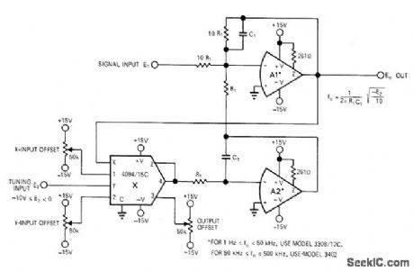
Coupling FET opamps with analog multiplierglves simple two-pole bandpass filter that canbe tuned by external voltage of 0-10 VDC to glve center frequency anywhere in range fromlHzto 500 kHz With components shown,Articleglves design equations,-T,Gate,Voltage Tune Your Bandpass Filters with Multipliers, EDN Magazine,March 1,1971,p 45-47. (View)
View full Circuit Diagram | Comments | Reading(547)
LOW_POWER_SCHMITT
Published:2009/7/2 20:32:00 Author:May

Uses two NAND gates from SN74L00 NAND package and one NOR gate (used as inverter) from CD4001AE CMOS package to make low-power Schmitt trigger. NAND gates are connected to form RS flip-flop. Q goes high when input voltage is greater than 2.1 V, and other output does not go low until input voltage is less than 1.2 V.Both polarities of output signal are available.-R. Cox, CMOS and LPTTL Gates Make LowPower Schmitt Trigger, EDN Magazine, Oct. 1, 1972,p48. (View)
View full Circuit Diagram | Comments | Reading(1778)
1_kHz_STATE_VARIABLE
Published:2009/7/2 20:31:00 Author:May
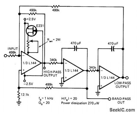
Low-power filter uses three opamps to provide simultaneous high-, low-, and bandpass outputs. Article presents complete design procedure for keeping current drain at minimum while providing desired gain-bandwidth product of 240 kHz.-L.Schaeffer, Op-Amp Active Filters-Simple to Design Once You Know the Game, EDN Magazine, April 20, 1976, p 79-84. (View)
View full Circuit Diagram | Comments | Reading(480)
EXCLUSIVE_OR_LOGIC_FOR_MUTING
Published:2009/7/2 20:28:00 Author:May
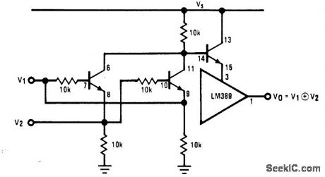
Connection shown for National LM389 combination ofthree transistors with opamp gives standard EXCLUSIVE-OR circuit for controlling muting transistor in audio system,Shorting pin 12 ofopamp to ground gives EXCLUSIVE-NORlogic.- Audio Handbook, National Semicondqctor,Santa Clara,CA,1977,p4-33-4-37 (View)
View full Circuit Diagram | Comments | Reading(585)
Basic_V_F_converter
Published:2009/7/24 1:48:00 Author:Jessie

Pig. 12-31 This circuit uses an XR4151 and a few external components to form a basic V/F converter. Using the values shown, input voltage is from 0 to + 10V, and output frequency is from 0 to 10 kHz. Full-scale frequency is trimmed by RS. EXAR Corporation Databook 1990 p 5-123.
(View)
View full Circuit Diagram | Comments | Reading(2324)
Step_down_P_channel_controllers
Published:2009/7/24 1:48:00 Author:Jessie


Figure 7-42 shows the MAX747 connected to provide +5 V at 2.3 A with a 7.5-V to 15-V input. Figure 7-43 shows the MAX747 connected to provide +3.3 V at 2.3 A with a 4.5-V to 15-V input. Figure 7-44 shows the calculations required for the low-battery detector circuit. LBO goes low when V+ is equal to or less than VTRIP. LBO is high impedance in the shutdown mode. Figure 7-45 shows the calculations required to adjust the output from 2 V to 14 V. The value of C6 is calculated using:where C1 is the value of C1 in μF, and ESRC1 (effective series resistance of C1 at 100 kHz) is in ohms. Figure 7-46 shows the recommended Kelvin connections for the current-sense resistor. MAXIM NEW RELEASES DATA Book, 1994, P. 4-140, 4-143, 4-145.
(View)
View full Circuit Diagram | Comments | Reading(650)
Micropower_V_F_converter_1_MHz
Published:2009/7/24 1:47:00 Author:Jessie

Fig. 12-30 In this circuit, a 0- to 5-V input produces a 100-Hz to 1-MHz output with a linearity of 0.02%. Drift is about 50 ppm/℃. Maximum current consumption (at 1 MHz) is about 360μA. To trim, apply 500μV and select a value (typically 240 kΩ) at the A1noninverting input for a 100-Hz output. Then, apply 5 V and adjust the 50-kΩ trim for a 1-MHz output. Then, apply 5 V and adjust the 50-kΩ trim for a 1-MHz output. Linear Technology. Linear Applications Handbook 1990 p AN23-13. (View)
View full Circuit Diagram | Comments | Reading(672)
FET_D_C_MILLIVOLTMETER_1
Published:2009/7/24 1:47:00 Author:Jessie

Consists of two circuits much like bootstrapped source-follower, differentially connected and fed by active current source. Input of 50 my produces full-scale defection, making sensitivity 20 meg/v.-L. J. Sevin, Jr., Field-Effect Transistors, McGraw-Hill, N.Y., 1965, p 110. (View)
View full Circuit Diagram | Comments | Reading(661)
ECL_INTERFACE_FOR_VMOS
Published:2009/7/2 20:22:00 Author:May
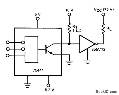
S55V12 VMOS (identical to S55V01 except for higher breakdown/saturation voltage) is used to buffer ECL-compatible SN75441 peripheral driver. Combination is capable of handling up to 90 V at 2 A.SN75441 has open-collector output, so inter-face with VMOS requires only pull-up resistor R1.-L. Shaeffer, VMOS Peripheral Drivers Solve High Power Load Interface Problems, Computer Design, Dec. 1977, p 90, 94, and 96-98. (View)
View full Circuit Diagram | Comments | Reading(1086)
Single_cell_voltage_up_converter
Published:2009/7/24 1:46:00 Author:Jessie

This circuit will supply a 5-V 150-μA load (about 25 CMOS SSI ICs, for example) for 3000 hours from a single 1.5-V D-cell battery. (View)
View full Circuit Diagram | Comments | Reading(553)
CMOS_INTERFACE_USING_OPTOlSOLATOR
Published:2009/7/2 20:18:00 Author:May

Provides logic control of 350-mA lamp. High level on input of typical CMOS inverter energizes 4N25 optoisolator, to clamp Q1 off. This removes drive from Q2, deenergizing load.Logic 0 at input reverses conditions, tuming on lamp. With values shown, 10 mA at optoisolator input controls completely isolated 350-mA load.-A. Pshaenich, Interface Techniques Between lndustrial Logic and Power Devices, Motorola, Phoenix, AZ, 1975, AN-712A, p 16. (View)
View full Circuit Diagram | Comments | Reading(2152)
POWER_ON_RESET
Published:2009/7/2 20:13:00 Author:May

One Schmitt trigger and three discrete components ensure correct initial state of logic circuits when power is applied.During charge time of C1, output of gate G1 is high. When C1 reaches 1.5V, gate output goes low and terminates power-on reset.-R. C. Snyder, Single-Voltage Circuit Generates Power-On Reset Pulse, EDNIEEE Magazine, Jan. 1, 1972, p 72. (View)
View full Circuit Diagram | Comments | Reading(0)
LEVEL_AND_POLARITY_SHIFTER
Published:2009/7/2 20:09:00 Author:May
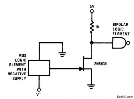
Simple FETcircuit provides for level shifting from MOS logic element having negative supply to TTL orother bipolar logic level operating from positivesupply and ground. Transistor has fast switching time.- FET Databook, National Semiconductor, Santa Clara, CA, 1977, p 6-26-6-36. (View)
View full Circuit Diagram | Comments | Reading(481)
95_MHz_TUNABLE_CRYSTAL
Published:2009/7/2 9:27:00 Author:May

Clapp oscillator with inductance in series with crystal can be tuned with C2 as much as 100 kHz below rated frequency of crystal. Based on making crystal act as capacitive reactance below its series-resonant frequency. Circuit can be adapted to other amateur bands by keeping reactances of various components approximately the same.-L. Lisle, The Tunable Crystal Oscillator, QST, Oct. 1973, p 30-32. (View)
View full Circuit Diagram | Comments | Reading(1095)
15_65_MHz_IMPEDANCE
Published:2009/7/2 9:26:00 Author:May
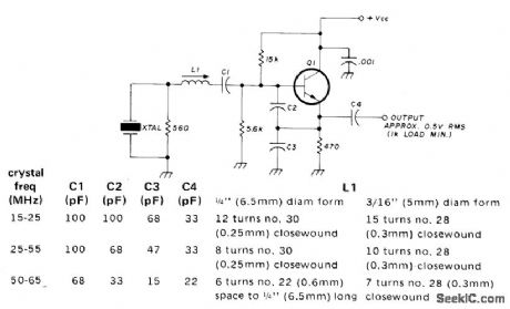
INVERTING-Uses third-overtone crystals. L1 trims crystal frequency. Resistor across crustal prevents oscillation at undesired modes. Starting is reliable and stability is good. Q1 is 2N3563, 2N3564, 2N5770, BF180, BF200, or SE1010.-R.Harrison, survey of Crystal Oscillators, Ham Radio, March 1976, p 10-22. (View)
View full Circuit Diagram | Comments | Reading(1296)
100_Hz_BANDPASS_SALLEN_KEY
Published:2009/7/2 9:25:00 Author:May
Uses one section of OP-11FY quad opamp or equivalent in circuit having Q of 4.7 and providing closed-loop gain of 200 or 46 dB. Opamp selected should have open-loop gain of 5 to 10 times required gain at resonance. Adiust resistor values to tune centerfrequency.-D. Van Dalsen, Need an Active Filter? Try These Design Aids, EDN Magazine, Nov.5, 1978, p 105-110.
(View)
View full Circuit Diagram | Comments | Reading(746)
10_MHz_VFO
Published:2009/7/2 9:25:00 Author:May

Values shown for high-stability variable-frequency oscillator give operation in 10-MHz range. Stable supply voltage is essential. Use silver mica capacitors in gate circuit for maximum stability.-E.M. Noll, FET Principles Experiments, and Projects, Howard W. Sams, Indianapolis, IN, 2nd Ed., 1975, p 193-194. (View)
View full Circuit Diagram | Comments | Reading(1335)
465_kHz_FOR_IF_TUNE_UP
Published:2009/7/2 9:24:00 Author:May

Simple crystal oscillator using National LM3909N is adjusted to exactly desired frequency with capacitor in series with pin 8. Drain from AA cell is less than 0.5 mA at 1.2 V. Use 465-kHz crystal and couple oscillator to receiver input with 100-pF capacitor. With 100-kHz crystal, circuit will generate strong harmonics beyond 30 MHz; to zero-beat with WWV, use about 10 pF in series with erystal.-I. Queen, Simple Crystal Oscillator, Ham Radio, Nov, 1977, p 98. (View)
View full Circuit Diagram | Comments | Reading(1290)
51_55_MHz
Published:2009/7/2 9:24:00 Author:May
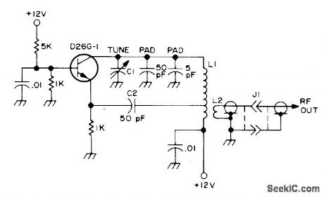
Tunable local oscillator is padded to tune over range required for use with 1.65-MHz IF in G.meter receiver, using Johnson type U 14-plate tuning capacitor. Can also serve as test transmitter putting out up to 20 mW. L1 is 9 tums No. 26 tapped 1 tum from low end, and L2 is 1 or 2 turns. Article covers constluction in 1 1/4 × 1 1/4 × 1/2 inch box.-B. Hoisington, A Real Hot Ftont End for Six, 73 Magazine, Nov. 1974, p 88-90 and 92-94. (View)
View full Circuit Diagram | Comments | Reading(546)
5_55_MHz_VFO
Published:2009/7/2 9:23:00 Author:May

Used in solid-state five-band communication receiver. Temperature compensation is provided by 20-pF trimmer that sets band center L1 is 34 turns No.24 on Amidon T50-6 toroid core.-P. Moroni, Solid-State Communications Receiver Ham Radio, Oct,1975, P 32-41 (View)
View full Circuit Diagram | Comments | Reading(1957)
| Pages:1137/2234 At 2011211122112311241125112611271128112911301131113211331134113511361137113811391140Under 20 |
Circuit Categories
power supply circuit
Amplifier Circuit
Basic Circuit
LED and Light Circuit
Sensor Circuit
Signal Processing
Electrical Equipment Circuit
Control Circuit
Remote Control Circuit
A/D-D/A Converter Circuit
Audio Circuit
Measuring and Test Circuit
Communication Circuit
Computer-Related Circuit
555 Circuit
Automotive Circuit
Repairing Circuit