
Circuit Diagram
Index 1145
SWITCHED_CRYSTALS
Published:2009/7/2 7:28:00 Author:May

High stability is combined with multichannel selection by diode switching of crystals in range of 2-20 MHz, used in series-resonant mode. L1 is about 30 μH at 2 MHz and 1 μH at 20 MHz. Q1 is 2N708, HEP50, BC108, or similar NPN RF type Diodes are switching types such as BAY67.-U. Rohde, Stable Crystal Oscillators, Ham Radio, June 1975, p 34-37. (View)
View full Circuit Diagram | Comments | Reading(1171)
JFET_PIERCE_CRYSTAL
Published:2009/7/2 7:27:00 Author:May

Basic JFET oscillatorcircuit permits use of wide frequency range of crystals. High Q is maintained because JFET gate does not load crystal, thereby ensuring good frequency stability.- FET Databook, National Semiconductor, Santa Clara, CA, 1977, p 6-26-6-36. (View)
View full Circuit Diagram | Comments | Reading(818)
42667_MHz_MOSFET
Published:2009/7/2 7:26:00 Author:May
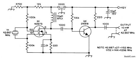
Unusual crystal-controlled oscillator, similar to modified Pierce oscillator that uses crystal between grids 1 and 2 of tetrode tube, can be used as local oscillator in VHF and UHF converters. No trimming ortuning is required to get overtone frequency. If fundamental of crystal is desired, increase RFC1 to 100 μH or replace it with 1K resistor. Stability is excellent. Circuit works well with supply as low as 4 V.-G. Tomassetti, Dual-Gate MOSFET Offers an Unusual Crystal-Controlled Oscillator Concept, QST, June 1976, p 39. (View)
View full Circuit Diagram | Comments | Reading(788)
SSB_CW_NOISE_LlMlTER
Published:2009/7/2 7:25:00 Author:May

Simple Iimiter is easy to install in receiver having good product detector. In place of dual-diode tube, semiconductor diodes having high front-to-back ratio may be used.-Novice Q & A. 73 Magazine. Holiday issue 1976 p 20. (View)
View full Circuit Diagram | Comments | Reading(648)
12_MC_CRYSTAL_STANDING_WAVE_DETECTOR
Published:2009/7/24 2:17:00 Author:Jessie

Transistorized crystal oscillator Q1 and emitter-follower Q2 feed 1 V rms into two balanced transmission lines going to standing-wave detector.-O. C. Haycock, and K. D. Baker, Measuring Antenna Impedance in the lonosphere, Electronics, 34:2, p 88-92. (View)
View full Circuit Diagram | Comments | Reading(504)
EMERGENCY_NOISE_GENERATOR
Published:2009/7/2 7:22:00 Author:May

Simple circuit generates noise in audio range at wideband level adjustable with 1 K pot from 0 to over 1 V. lf 680-pF capacitor is omitted, noise output goes up to 30 MHz with wideband level more than 5 V.-D. Di Mario. Simple Noise Generator. Wireless World. May 1978. p 70. (View)
View full Circuit Diagram | Comments | Reading(1644)
9_V_high_efficiency_controller
Published:2009/7/24 2:17:00 Author:Jessie

Figure 7-53 shows the MAX1771 connected to provide 9-V output with a 4-V input. See Fig. 7-51 for component suppliers.AXIM NEW RELEASES DATA BOOk, 1995.P4-20. (View)
View full Circuit Diagram | Comments | Reading(631)
Micropower_sample_hold
Published:2009/7/24 2:17:00 Author:Jessie

This sample-hold circuit has an acquisition time of 20 μS, with a hold-current of 430 μA, and a sample-current of 2.2 mA. (View)
View full Circuit Diagram | Comments | Reading(608)
AF_NOISE_LlMITER
Published:2009/7/2 7:17:00 Author:May

Audio signals rectified by diodes develop bias across R1 and C1 such that diodes are back-biased. Diodes thus conduct and clip only when noise signal peaks exceed bias level.Component values depend on impedance of audio circuit;table gives values for thre common load resistors. Diodes are fast-switching silicon such as 1 N 916. To minimize residual clipping distortion. use value for CF that gives 3-dB rolloff at about 2.5 kHz.-P. Lovelock. The Audio Bishop. 73 Magazine. Sept. 1974. p 75-76 (View)
View full Circuit Diagram | Comments | Reading(670)
PRECISION_R_C_OSCILLATOR
Published:2009/7/24 2:17:00 Author:Jessie

Used in signal generator for testing systems by varying frequency over very small limits, as in aligning filters having sharp resonance curves. Cathode follower V2 is included in feedback loop to reduce loading on bridge network. Covers 25 cps to 250 kc in four ranges, with incremental control giving increment of 2% of maximum frequency in each range.-J. H. Reyner, Precision Oscillator with Incremental Tuning, Electronics, 33:16, p 76-78. (View)
View full Circuit Diagram | Comments | Reading(910)
3955_4455_MHz_VFO
Published:2009/7/2 7:12:00 Author:May
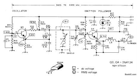
Basic Colpitts LC oscillator designed for 80-meter receivel wiith 455-kHz IF uses zener in supply line to minimize frequncy drift. Emitter-follower buffer contributes to stability by isolating oscillator frommlxer Low-pass filter C13-L2-C14 attenuates harmonic currents developed in Q3 and Q4. L1 is Miller 4503 1.7-2.7 μH variable inductor. L2 is 48 turns No.30 enamel closewound on 1/4-inch wood dowel or polystyrene rod. Main tuning capacitor C10 can be 365-pF unit with six of rear rotor plates removed.-D. DeMaw and L. McCoy, Learning to Work with Semiconductors, QST, June 1974, p 18-22 and 72. (View)
View full Circuit Diagram | Comments | Reading(2022)
INDUSTRIAL_BRAZING_CIRCUIT
Published:2009/7/24 2:17:00 Author:Jessie

Applies high r-f power peaks in short-duration pulses, such as 11 kw for 2 sec or 45 kw for 0.5 sec, repeated every 5 sec. Settings of time delay relays RE1 and RE2 determine pulse lengths.-J. Markus and V. Zeluff, Handbook of Industrial Electronic Control Circuits, McGraw-Hill, New York, 1956, p 340. (View)
View full Circuit Diagram | Comments | Reading(636)
1O_2O_MHz_CRYSTAL
Published:2009/7/2 7:11:00 Author:May

Modification of basic Colpitts crystal oscillator has excellent load capacitance correlationand temperature stability. Crystal will oscillate very close to its series resonant point. Component values are optimized for 10-20 MHz. Emitter-follower Q2 provides power gain for feedback energy and gives high crystal activity without changing phase angle of signal. Output buffer Q3 prevents loading of oscillator. Q1 is low-cost Motorola JFET, but practically any other JFET will work CR1 is 1N914 or 1N4148.-D. L. Stoner, High-Stability Crystal Oscillator, Ham Radio, Oct. 1974, p 36-39. (View)
View full Circuit Diagram | Comments | Reading(1442)
UP_TO_30MHz
Published:2009/7/2 7:10:00 Author:May

Simple single-transistor PF oscillator is easily assembled from noncritical parts, Tuning capacitor and coil determine frequency.-Circuits, 73 Magazine, July 1977, p 35. (View)
View full Circuit Diagram | Comments | Reading(631)
GENERAL_PURPOSE_UP_TO_10_MHz
Published:2009/7/2 7:09:00 Author:May

Variation of Colpitts oscillator uses negative feedback at all frequencies at which LC network does not provide phase inversion and voltage step-up.Choose values for coil and capacitors to give frequency desired. R3 serves as regeneration control and for changing waveform of output.-G. W. Short, Good-Tempered LC Oscillator, Wire-less World, Feb. 1973, p 84. (View)
View full Circuit Diagram | Comments | Reading(650)
GATED_5_MHz_RELAXATION
Published:2009/7/2 7:03:00 Author:May
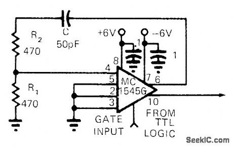
Output always startsVin same phase with respect to gating signal. Frequency-selective network R1-R2-C provides positive feedback around MC15456 gatecontrolled wideband amplifier.-F.Macli, IC Op Amp Makes Gated Oscillator, EDN Magazine,Sept. 1, 1972, p 52. (View)
View full Circuit Diagram | Comments | Reading(468)
1_20_MHz_FUNDAMENTAL_CRYSTAL
Published:2009/7/2 7:02:00 Author:May

Oscillator requires no resonant tank circuit for frequencies below 20 MHz. Use of noninverting output makes oscillator section of Motorola MC10116 IC function simply as amplifier. Second section is connected as Schmitt trigger to improve signal waveform. Third section is buffer providing complementary outputs.-B. Blood, IC Crystal Controlled Oscillators, Motorola, Phoenix, AZ, 1977, AN-417B, p 4. (View)
View full Circuit Diagram | Comments | Reading(766)
SPIKE_REJECTlON
Published:2009/7/2 5:33:00 Author:May
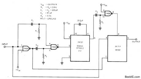
Used to eliminate noise that may be present on signal Iine. Based on sampling input Iine at fixed time after each detected transition. If transition was due to noise spike, spike will no longer be present and true signal level will be sampled. lf transition was caused by desired legitimate signal, sampled waveform represents true signal delayed by pulse width of mono MVBR. Mono pulse width is about 12μs. Article gives circuit waveforms and describes operation in detail.-A. S. Bozorth, Pulse Verification Yields Good Noise Immunity. EDN Magazine. Nov. 5. 1973. p 75 and 77. (View)
View full Circuit Diagram | Comments | Reading(637)
TTL_INrERFACE
Published:2009/7/2 5:31:00 Author:May
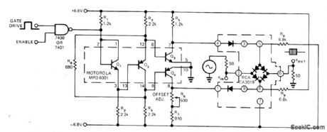
MotoroIa MPQ 6001 quad complementary-pair transistor IC serves as interface between TTL gateand diodebrldge used as signal gate. Propagation delay from leadingedge of gate drive pulse until bridge gate opens is 30 ns, with negligible delay between complementary outputs. Used in providing low-level burst of input signal when making response ime measurement.-R. W. Hilsher, Universal Interface: TTL to Diode Array, EDN Magazine, March 5, 1975, p 74 and 76, (View)
View full Circuit Diagram | Comments | Reading(580)
Simple_differential_thermometer
Published:2009/7/24 2:16:00 Author:Jessie

Fig. 13-12 This circuit produces an output voltage that is proportional to the temperature difference between the two LM34s. The difference amplifier sub-tracts the LM34 outputs from one another and then multiplies the difference by a factor of 10 to provide a single-ended output of 100 mV/°F of differential temperature. National Semiconductor Linear Applications Handbook 1991, p 1079. (View)
View full Circuit Diagram | Comments | Reading(632)
| Pages:1145/2234 At 2011411142114311441145114611471148114911501151115211531154115511561157115811591160Under 20 |
Circuit Categories
power supply circuit
Amplifier Circuit
Basic Circuit
LED and Light Circuit
Sensor Circuit
Signal Processing
Electrical Equipment Circuit
Control Circuit
Remote Control Circuit
A/D-D/A Converter Circuit
Audio Circuit
Measuring and Test Circuit
Communication Circuit
Computer-Related Circuit
555 Circuit
Automotive Circuit
Repairing Circuit