
Circuit Diagram
Index 1161
1Hz_TO_10_MHz
Published:2009/7/2 0:32:00 Author:May

Simple circuit operating from single 5-V supply provides TTL output levels with reliable starting over wide frequency range. When capacitors are equal, period of oscillation is equal to 5×10³C s. By changing ratio of C1 to C2, duty cycle can be made as low as 20%.-D. B. Arnett, One-Chip TTL Oscillator Requires One 5V Supply, EDN Magazine, Jan. 5, 1978, p 96. (View)
View full Circuit Diagram | Comments | Reading(909)
BASIC_MONO_DRIVES_LED
Published:2009/7/2 0:31:00 Author:May

Two sections of 7400 quad NAND gate are connected as monostable MVBR having one stable state and one unstable state. Incoming pulse at pin 13 changes state of gate IC1. Since output of this gate goes to input of other gate, that also changes state. After interval determined by values of C1 and R1, gates automatically return to original states. LED flashes when input pulse is applied, for duration also determined by R1 or C1. If C1 is increased to 470μF, LED will stay on for over 1 s before fading out gradually as capacitor discharges.-F. M. Mints, Integrated Circuit Projects, Vol. 2, Radio Shack, Fort Worth, TX, 1977, 2nd Ed., p 19-26. (View)
View full Circuit Diagram | Comments | Reading(1299)
MONO_SQUARE_WAVE
Published:2009/7/2 0:30:00 Author:May

Stable characteristics of differential amplifier in CA3080 variable opamp assure pre be timing and threshold for output waveform. Opamp drives one inverter/amplifier section of CA3600E inverter array. Supply voltage range is ±3 to± 15V.- Circuit Ideas for RCA Linear ICs, RCA Solid State Division, Somerville, NJ, 1977, p 5. (View)
View full Circuit Diagram | Comments | Reading(490)
SQUARE_WAVE_BURSTS
Published:2009/7/2 0:29:00 Author:May

When pushbutton switch is closed, 555 timer generates square-wave tone bursts for duration depending on how long voltage on pin 4 exceeds threshold value. R1, R2, and C, control astable action of timer.- Signetics Analog Data Manual, Signetics, Sunnyvale, CA, 1977, p 726. (View)
View full Circuit Diagram | Comments | Reading(525)
ASYMMETRICAL_SQUARE_WAVES
Published:2009/7/2 0:28:00 Author:May

Addition of D1 and R4 to astable MVBR connection of 741 or equivalent opamp results in two different charging rates for C1, depending on whether opamp is in positive or negative saturation. Positive and negative peaks of output pulse then have different widths.-R. Melen and H. Garland, Understanding IC Operational Amplifiers, Howard W. Sams, Indianapolis, IN, 2nd Ed., 1978, p 122-123. (View)
View full Circuit Diagram | Comments | Reading(614)
FREE_RUNNING
Published:2009/7/2 0:27:00 Author:May

Positive feedback is applied to noninverting input terminal of oparnp through voltage divider R1-R2 to make amplifier switch regeneratively and repetitively between saturated states. Charging time of C controls duration of each state, to give desired free-running multivibrator providing rectangular (pin 6), trapezoidal (pin 3), and sawtooth (pin 2) sym-metrical waveforms. Article gives design equations and waveforms. For nonsymmetrical waveforms, use alternative circuit in place of R; here, diodes switch two different timing resistors into circuit alternately.-G. B. Clayton, Experiments with Operational Amplifiers, Wire-less World, May 1973, p 241-242. (View)
View full Circuit Diagram | Comments | Reading(625)
ASTABLE_SQUARE_WAVE
Published:2009/7/2 0:26:00 Author:May

CA3080 variable opamp drives one inverter/amplifier section of CA3600E inverter array. Quiescent power drain is typically 6 mW. Supply voltage range is ±3 to ±15V.- Circuit Ideas for RCA Linear ICs, RCA Solid State Division, Somerville, NJ, 1977, p 5. (View)
View full Circuit Diagram | Comments | Reading(511)
SEQUENTIAL_TIMING_GIVES_DELAYED_MONO_MVBR
Published:2009/7/2 0:25:00 Author:May

Output of first timer section of Exar XR-2556 dual timer is capacitively coupled to trigger pin of second timer section. When input trigger is applied, output 1 goes high for duration T1 = 1.1R1C1, then goes low and triggers timer 2 through CC. Output at pin 13 then goes high for duration T2 = 1.1R2C2 to give performance of delayed mono MVBR. Supply voltage is 4.5-16 V. Choose R, to keep timer output below 200 mA for supply voltage used.- Timer Data Book, Exar Integrated Systems, Sunnyvale, CA, 1978, p 23-30. (View)
View full Circuit Diagram | Comments | Reading(525)
PULSE_WIDTH_CONTROL
Published:2009/7/2 0:24:00 Author:May

DC input voltage controls width of rectangular output pulse of opamp operating as free-running multivibrator, by injecting additional current into phase-inverting input of opamp. This current serves to increase one timing period and decrease the other. Circuit also provides similarly controllable sawtooth output (at pin 2). Output circuit uses diode bridge and zener for symmetrically clamping output voltage limits of amplifier when this feature is required.-G. B. Clayton, Experiments with Operational Amplifiers, Wire-less World, May 1973, p 241-242. (View)
View full Circuit Diagram | Comments | Reading(623)
GATED_ASTABLE
Published:2009/7/2 0:24:00 Author:May
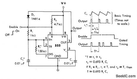
With values shown, circuit produces positive output pulses at about 1 kHz when gated on by positive pulse at pin 4. Supply voltage for 555 timer can be 15V.-W. G. Jung, IC Timer Cookbook, Howard W. Sams, Indianapolis, IN, 1977, p 135-136. (View)
View full Circuit Diagram | Comments | Reading(981)
455_Hz_ASTABLE
Published:2009/7/2 0:23:00 Author:May

Frequency of square-wave output depends on values used for external capacitor and resistors. Very low frequencies can be obtained by using large values for both. High-frequency performance is limited by slew rate of opamp.-R. Melen and H. Garland, Understanding IC Operational Amplifiers, Howard W. Sams, Indianapolis, IN, 2nd Ed., 1978, p 119-120. (View)
View full Circuit Diagram | Comments | Reading(500)
HIGH_PRECISION_F_V_1
Published:2009/7/2 0:03:00 Author:May
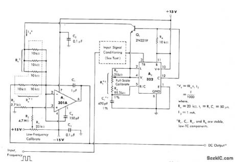
Components of V/F converter are reconnected to provide F/ V function.Inputfrequency up to 10 kHz is fed to 322 mono MVBR A2, either directly if pulsed or indirectly after conditioning. For low-frequency or slowly changing waveforms, zero crossing detector is used forinρut conditioning,A1isconnected asscaling amplifier and filter.-W. G .Jung, ''IC Timer Cookbook,″Howard W .Sams、lndianapoils,IN,1977,ρ 192-196. (View)
View full Circuit Diagram | Comments | Reading(499)
POSITIVE_INPUT_GIVES_GREEN
Published:2009/7/1 23:58:00 Author:May
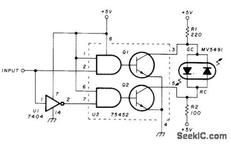
High or positive input to circuit gives green indication in Monsanto MV5491 dual red/green LED, and low input gives red. Circuit uses single SN75452 IC INPUT driver and one section of SN7404 hex nverter.-K. Powell, Novel Indicator Circuit,Ham Radio, April 1977, p 60-63. (View)
View full Circuit Diagram | Comments | Reading(656)
PIANO_TUNING_AMPLIFIER
Published:2009/7/1 23:58:00 Author:May
Used with battery-powered digital tuning aid that provides 12 equal semitones of octave, between 261.6625 and 493.8833 Hz, for equal-temperamenttuning of such keyboard instruments as organ. piano. and harpsichord. IC used is part of RCA amplifier kit KC-4003 which includes T1 and other discrete components. Article gives circuits for oscillator and programmable divider, along with instructions for construction. calibration. and use.-W.S. Pike. Digital Tuning Aid. Wireless World. July 1974. p 224-227. (View)
View full Circuit Diagram | Comments | Reading(671)
RF_SNIFFER
Published:2009/7/1 23:56:00 Author:May

This circuit responds to RF signals from below the standard broadcast band to well over 500 MHz, and provides a visual and audible indication when a signal is received.The circuit is designed to receive low-powered signals as well as strong sources of energy by adjusting the bias on the pick-up diode, D1, with R2. A very sensitive setting can be obtained by carefully adjusting R2 until the LED just begins to light and a faint sound is produced by the Piezo sounder. (View)
View full Circuit Diagram | Comments | Reading(1449)
STROBING_LED_DISPLAY_1
Published:2009/7/1 23:56:00 Author:May

Sequential strobing of individual LED displays, at rate fast enough to eliminate flicker (about 10% duty cycle), cuts power requirements of LEDs and eliminates need for power-wasting resistors in series with digit segments. Circuit uses 7492 binary counter connected to divide by 10, continuously clocked by 1000-Hz signal from external counter time base. Each of the 10 counter states is decoded by 7442 decoder for use in turning on PNP switch transistor connected in series with anode of each 7-segment LED digit. Digits are thus turned on fol 10'/0 of time at 100-Hz rate.-B. Hart, Current-Saver Counter Display, 73 Magazine, June 1977, p 174-176. (View)
View full Circuit Diagram | Comments | Reading(1316)
6_DIGIT_FOUR_FU_NCTION_1
Published:2009/7/1 23:54:00 Author:May

National MM5777 calculator chip requires only keyboard, NSA1161 LED display, DS8977 digit driver, and 9-V battery to provide add, subtract, multiply, and divide functions. Calculator chip includes keyboard encoding and key debouncing circuits, along with all clock and timing generators. LED segments can be driven directly, without multiplexing. Seventh digit position is used for negative sign of 6-digit number and as error indicator.Leading and trailing zero suppressionis included.-, MOS/LSI Databook, National Semiconductor,Santa Clara,GA,1977,p 8-84-8-89. (View)
View full Circuit Diagram | Comments | Reading(535)
FIELD_STRENGTH_METER_II
Published:2009/7/1 23:53:00 Author:May

Minimum-parts field-strength meter is shown here. For more distant testing, add the dc amplifier. (View)
View full Circuit Diagram | Comments | Reading(1160)
6_DIGIT_FOUR_FU_NCTION
Published:2009/7/1 23:52:00 Author:May
National MM5777 calculator chip requires only keyboard, NSA1161 LED display, DS8977 digit driver, and 9-V battery to provide add, subtract, multiply, and divide functions. Calculator chip includes keyboard encoding and key debouncing circuits, along with all clock and timing generators. LED segments can be driven directly, without multiplexing. Seventh digit position is used for negative sign of 6-digit number and as error indicator.Leading and trailing zero suppressionis included.-, MOS/LSI Databook, National Semiconductor,Santa Clara,GA,1977,p 8-84-8-89. (View)
View full Circuit Diagram | Comments | Reading(700)
GATE_DIP_FET_OSCILLATOR_
Published:2009/7/1 23:51:00 Author:May

Meter indicates gate current, which drops whenever resonant load is placed on tank circuit of oscillator by bringing plug-in input coil near frequency source being checked. By opening switch to power supply, circuit can be used as absorption wavemeter; when signal at resonant frequency of dip-meter tank circuit is picked up, gatesource circuit of FET operates as diode detector for producing increase in meter reading. Values of plug-in coil and tuning capacitor depend on frequency range of interest.-E. M. Noll, FET Principles, Experiments, and Projects, Howard W. Sams, Indianapolis, IN, 2nd Ed., 1975, p 213-214. (View)
View full Circuit Diagram | Comments | Reading(3449)
| Pages:1161/2234 At 2011611162116311641165116611671168116911701171117211731174117511761177117811791180Under 20 |
Circuit Categories
power supply circuit
Amplifier Circuit
Basic Circuit
LED and Light Circuit
Sensor Circuit
Signal Processing
Electrical Equipment Circuit
Control Circuit
Remote Control Circuit
A/D-D/A Converter Circuit
Audio Circuit
Measuring and Test Circuit
Communication Circuit
Computer-Related Circuit
555 Circuit
Automotive Circuit
Repairing Circuit